
Recherchez avec le numéro de pièce ainsi que le fabricant ou la description
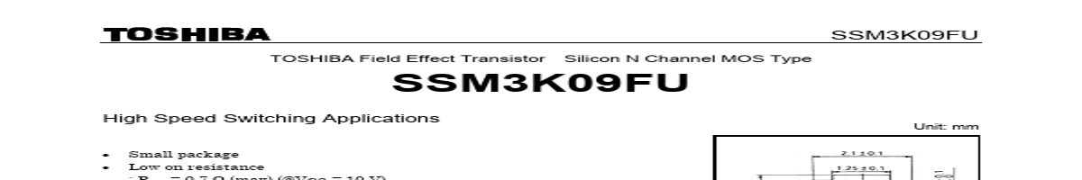
SSM3K09FU TOSHIBA Field Effect Transistor Silicon N Channel MOS Type SSM3K09FU High Speed Switching Applications Unit: mm • Small package • Low on resistance : Ron = 0.7 Ω (max) (@VGS = 10 V) : Ron = 1.2 Ω (max) (@VGS = 4 V) Absolute Maximum Ratings (Ta = 25°C) Characteristics Symbol Rating Unit Drain-Source voltage VDS 30 V Gate-Source voltage .
e reliability upon reviewing the Toshiba Semiconductor Reliability Handbook (“Handling Precautions”/“Derating Concept and Methods”) and individual reliability data (i.e. reliability test report and estimated failure rate, etc). Note 1: Mounted on FR4 board (25.4 mm × 25.4 mm × 1.6 t, Cu Pad: 0.6 mm2 × 3) Figure 1. Marking 3 DJ Equivalent Circuit (top view) 3 Figure 1: 25.4 mm × 25.4 mm × 1.6 t, Cu Pad: 0.6 mm2 × 3 0.6 mm 1.0 mm 1 2 1 2 Handling Precaution When handling individual devices (which are not yet mounting on a circuit board), be sure that the environment is protected agai.
| No. | Partie # | Fabricant | Description | Fiche Technique |
|---|---|---|---|---|
| 1 | SSM3K01F |

Toshiba Semiconductor |
Silicon N-Channel MOSFET |

|
| 2 | SSM3K01T |
Toshiba Semiconductor |
Silicon N-Channel MOSFET |
|
| 3 | SSM3K02F |
Toshiba Semiconductor |
TOSHIBA Field Effect Transistor Silicon N Channel MOS Type |
|
| 4 | SSM3K02T |
Toshiba Semiconductor |
High Speed Switching Applications |
|
| 5 | SSM3K03FE |
Toshiba Semiconductor |
Silicon N-Channel MOS Type FET |
|
| 6 | SSM3K03FV |
Toshiba Semiconductor |
High Speed Switching Applications |
|
| 7 | SSM3K03TE |
Toshiba Semiconductor |
High Speed Switching Applications |
|
| 8 | SSM3K04FE |
Toshiba Semiconductor |
High Speed Switching Applications |
|
| 9 | SSM3K04FS |
Toshiba Semiconductor |
Silicon N-Channel MOSFET |
|
| 10 | SSM3K04FU |
Toshiba Semiconductor |
High Speed Switching Applications |
|
| 11 | SSM3K04FV |
Toshiba Semiconductor |
High Speed Switching Applications |
|
| 12 | SSM3K05FU |
Toshiba Semiconductor |
Silicon N-Channel MOSFET |
|