
Recherchez avec le numéro de pièce ainsi que le fabricant ou la description
This 25-bit 1:1 or 14-bit 1:2 configurable registered buffer is designed for 1.7-V to 1.9-V VDD operation. All clock and data inputs are compatible with the JEDEC standard for SSTL_18. The control inputs are LVCMOS. All outputs are 1.8-V CMOS drivers that have been optimized to drive the DDR-II DIMM load. ICSSSTUB32866B operates from a differential clock (CK.
• 25-bit 1:1 or 14-bit 1:2 configurable registered buffer with parity check functionality
• Supports SSTL_18 JEDEC specification on data inputs and outputs
• Supports LVCMOS switching levels on CSR and RESET inputs
• Low voltage operation VDD = 1.7V to 1.9V
• Available in 96 BGA package
• Drop-in replacement for ICSSSTUA32864
• Green packages available
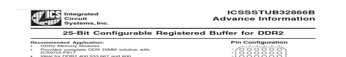
Pin Configuration
1 A B C D E F G H J K L M N P R T 2 3 4 5 6
Functionality Truth Table
Inputs RST H H H H H H H H H H H H L DCS CSR Dn, DODT, DCKE ↑ ↓ L ↑ ↓ H L or H L or H X ↑ ↓ L ↑ ↓ H L or H L or H X ↑ ↓ L ↑ ↓ H L or H L or H X ↑ ↓ L ↑ ↓ .
| No. | Partie # | Fabricant | Description | Fiche Technique |
|---|---|---|---|---|
| 1 | ICSSSTUB32864A |

ICS |
25-Bit Configurable Registered Buffer |

|
| 2 | ICSSSTUB32871A |
ICS |
27-Bit Registered Buffer |
|
| 3 | ICSSSTUB32872A |
ICS |
28-Bit Registered Buffer |
|
| 4 | ICSSSTUBF32866A |
ICS |
25-Bit Configurable Registered Buffer |
|
| 5 | ICSSSTU32864 |
ICS |
25-Bit Configurable Registered Buffer |
|
| 6 | ICSSSTU32866 |

Integrated Circuit System |
25-Bit Configurable Registered Buffer |
|
| 7 | ICSSSTUA32S869B |
ICS |
14-Bit Configurable Registered Buffer |
|
| 8 | ICSSSTUAF32865A |

IDT |
25-BIT CONFIGURABLE REGISTERED BUFFER |
|
| 9 | ICSSSTUAF32866B |
IDT |
25-BIT CONFIGURABLE REGISTERED BUFFER |
|
| 10 | ICSSSTUAF32866C |
IDT |
25-BIT CONFIGURABLE REGISTERED BUFFER |
|
| 11 | ICSSSTUAF32868A |
IDT |
28-BIT CONFIGURABLE REGISTERED BUFFER |
|
| 12 | ICSSSTUAF32868B |
IDT |
28-BIT CONFIGURABLE REGISTERED BUFFER |
|