
Recherchez avec le numéro de pièce ainsi que le fabricant ou la description
The PLL102 -15 is a high performance, low skew, low jitter zero delay buffer designed to di stribute high speed clocks and is available in 8 -pin SOIC or TSSOP package. It has four outputs that are synchronized with the input. The synchronization is established via CLKOUT feedback to the input of the PLL. Since the skew b etween the input and outpu t is les.
Frequency range 25 ~ 60MHz. Internal phase locked loop will allow spread spec trum modulation on reference clock to pass to the outputs (up to 33kHz SST modulation).
• Zero input - output delay.
• Less than 700 ps device - device skew.
• Less than 250 ps skew between outputs. www.DataSheet4U.com
• Less than 200 ps cycle - cycle jitter.
• Output Enable function tri -state outputs.
• 3.3V operation.
• Available in 8 -Pin 150mil SOIC.
•
•
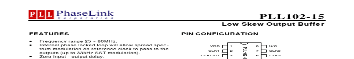
PIN CONFIGURATION
VDD CLK1 CLKOUT GND
1 2 3 4
8 7 6 5
N/C CLK3 CLK2 REF_IN
PLL102-15
Remark
If REF_IN clock is stopped for more than 10us after it has al.
| No. | Partie # | Fabricant | Description | Fiche Technique |
|---|---|---|---|---|
| 1 | PLL102-10 |

PhaseLink Corporation |
Low Skew Output Buffer |

|
| 2 | PLL102-108 |
PhaseLink Corporation |
Programmable DDR Zero Delay Clock Driver |
|
| 3 | PLL102-109 |
PhaseLink Corporation |
Programmable DDR Zero Delay Clock Driver |
|
| 4 | PLL102-03 |
PhaseLink Corporation |
Low Skew Output Buffer |
|
| 5 | PLL102-04 |
PhaseLink Corporation |
Low Skew Output Buffer |
|
| 6 | PLL102-05 |
PhaseLink Corporation |
Low Skew Output Buffer |
|
| 7 | PLL1000A |

Z-Communications |
PHASE LOCKED LOOP |
|
| 8 | PLL103-01 |
PhaseLink Corporation |
Low Skew Buffer |
|
| 9 | PLL103-02 |
PhaseLink Corporation |
DDR SDRAM Buffer |
|
| 10 | PLL103-03 |
PhaseLink Corporation |
DDR SDRAM Buffer |
|
| 11 | PLL103-04 |
PhaseLink Corporation |
1-to-4 Clock Distribution Buffer |
|
| 12 | PLL103-05 |
PhaseLink Corporation |
1-to-5 Clock Distribution Buffer |
|