
Recherchez avec le numéro de pièce ainsi que le fabricant ou la description
The PLL102-10 is a high performance, low skew, low jitter zero delay buffer designed to distribute high speed clocks and is available in 8-pin SOIC or MSOP package. It has two outputs that are synchronized with the input. The synchronization is established via CLKOUT feed back to the input of the PLL. Since the skew between the input and output is less than .
Frequency range 50 ~ 120MHz. Internal phase locked loop will allow spread spectrum modulation on reference clock to pass to outputs.
• Zero input - output delay.
• Less than 700 ps device - device skew.
• Less than 250 ps skew between outputs. www.DataSheet4U.com
• Less than 100 ps cycle - cycle jitter.
• 2.5V or 3.3V power supply operation.
• Available in 8-Pin SOIC or MSOP package.
•
•
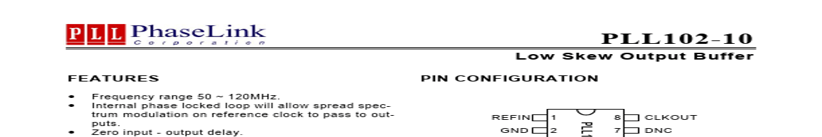
PIN CONFIGURATION
REFIN GND CLK1 CLK2
1
8
CLKOUT DNC DNC VDD
PLL102-10
2 3 4
7 6 5
DESCRIPTION
The PLL102-10 is a high performance, low skew, low jitter zero delay buffer designed to distribute high s.
| No. | Partie # | Fabricant | Description | Fiche Technique |
|---|---|---|---|---|
| 1 | PLL102-108 |

PhaseLink Corporation |
Programmable DDR Zero Delay Clock Driver |

|
| 2 | PLL102-109 |
PhaseLink Corporation |
Programmable DDR Zero Delay Clock Driver |
|
| 3 | PLL102-15 |
PhaseLink Corporation |
Low Skew Output Buffer |
|
| 4 | PLL102-03 |
PhaseLink Corporation |
Low Skew Output Buffer |
|
| 5 | PLL102-04 |
PhaseLink Corporation |
Low Skew Output Buffer |
|
| 6 | PLL102-05 |
PhaseLink Corporation |
Low Skew Output Buffer |
|
| 7 | PLL1000A |

Z-Communications |
PHASE LOCKED LOOP |
|
| 8 | PLL103-01 |
PhaseLink Corporation |
Low Skew Buffer |
|
| 9 | PLL103-02 |
PhaseLink Corporation |
DDR SDRAM Buffer |
|
| 10 | PLL103-03 |
PhaseLink Corporation |
DDR SDRAM Buffer |
|
| 11 | PLL103-04 |
PhaseLink Corporation |
1-to-4 Clock Distribution Buffer |
|
| 12 | PLL103-05 |
PhaseLink Corporation |
1-to-5 Clock Distribution Buffer |
|