
Recherchez avec le numéro de pièce ainsi que le fabricant ou la description
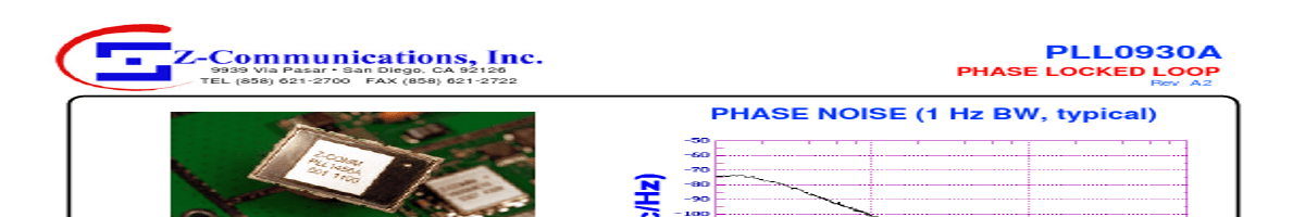
NOTES: Reference Oscillator Signal: 5 MHz< f o s c <40 MHz www.DataSheet4U.com www.DataSheet4U.com © Z-Communications, Inc. Page 1 All rights reserved LOW COST - HIGH PERFORMANCE PHASE LOCKED LOOP PLL OUTPUT SPECTRUM 0 -10 -20 -30 PLL0930A PAGE 2 POWER -40 -50 -60 -70 -80 -90 -100 -5 -4 -3 -2 -1 930 MHz +1 +2 +3 +4 +5 FREQUENCY OFFSET (KHz) POWER CU.
• Frequency Range: 900 - 960 MHz
• Step Size: 100 KHz
• PLL - Style Package APPLICATIONS
• Basestations
• Mobile Radios
• Satellite Communications PERFORMANCE SPECIFICATIONS
Frequency Range RMS Phase Error (100 Hz - 100 KHz) Harmonic Suppression (2nd, typ.) Sideband Spurs (typ.) Power Output Load Impedance Step Size Charge Pump Output Current Switching Speed (typ., adjacent channel) Startup Lock Time (typ.) Operating Temperature Range Package Style
VALUE 900 - 960 0.75 -15 -65 3±2 50 100 HIGH 1 5 -40 to +85 PLL
UNITS MHz ° dBc dBc dBm
Ω
KHz mSec mSec °C
POWER SUPPLY REQUIREMENTS
Supply Vol.
| No. | Partie # | Fabricant | Description | Fiche Technique |
|---|---|---|---|---|
| 1 | PLL0210A |

Z-Communications |
PHASE LOCKED LOOP |

|
| 2 | PLL1000A |
Z-Communications |
PHASE LOCKED LOOP |
|
| 3 | PLL102-03 |

PhaseLink Corporation |
Low Skew Output Buffer |
|
| 4 | PLL102-04 |
PhaseLink Corporation |
Low Skew Output Buffer |
|
| 5 | PLL102-05 |
PhaseLink Corporation |
Low Skew Output Buffer |
|
| 6 | PLL102-10 |
PhaseLink Corporation |
Low Skew Output Buffer |
|
| 7 | PLL102-108 |
PhaseLink Corporation |
Programmable DDR Zero Delay Clock Driver |
|
| 8 | PLL102-109 |
PhaseLink Corporation |
Programmable DDR Zero Delay Clock Driver |
|
| 9 | PLL102-15 |
PhaseLink Corporation |
Low Skew Output Buffer |
|
| 10 | PLL103-01 |
PhaseLink Corporation |
Low Skew Buffer |
|
| 11 | PLL103-02 |
PhaseLink Corporation |
DDR SDRAM Buffer |
|
| 12 | PLL103-03 |
PhaseLink Corporation |
DDR SDRAM Buffer |
|