
Recherchez avec le numéro de pièce ainsi que le fabricant ou la description
The 14-bit ICSSSTVA16857 is a universal bus driver designed for 2.3V to 2.7V VDD operation and SSTL_2 I/O levels, except for the LVCMOS RESET# input. Data flow from D to Q is controlled by the differential clock (CLK/CLK#) and a control signal (RESET#). The positive edge of CLK is used to trigger the data flow and CLK# is used to maintain sufficient noise ma.
• Exceeds "SSTVN16857" performance
• Differential clock signal
• Meets SSTL_2 signal data
• Supports SSTL_2 class I & II specifications
• Low-voltage operation - VDD = 2.3V to 2.7V
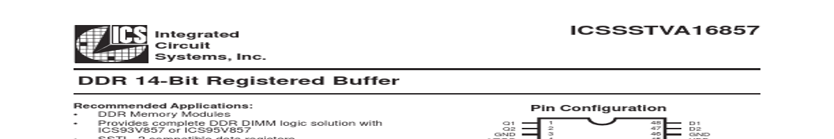
• 48 pin TSSOP package
Pin Configuration
Q1 Q2 GND VDDQ Q3 Q4 Q5 GND VDDQ Q6 Q7 VDDQ GND Q8 Q9 VDDQ GND Q10 Q11 Q12 VDDQ GND Q13 Q14 1 2 3 4 5 6 7 8 9 10 11 12 13 14 15 16 17 18 19 20 21 22 23 24 48 47 46 45 44 43 42 41 40 39 38 37 36 35 34 33 32 31 30 29 28 27 26 25 D1 D2 GND VDD D3 D4 D5 D6 D7 CLK# CLK VDD GND VREF RESET# D8 D9 D10 D11 D12 VDD GND D13 D14
Truth Table1
Inputs RESET# L H H H
Notes: 1. H = High Si.
| No. | Partie # | Fabricant | Description | Fiche Technique |
|---|---|---|---|---|
| 1 | ICSSSTVA16859B |

Integrated Circuit Systems |
DDR 13-Bit to 26-Bit Registered Buffer |

|
| 2 | ICSSSTVA16859C |

Renesas |
DDR 13-Bit to 26-Bit Registered Buffer |
|
| 3 | ICSSSTVA16859C |

IDT |
DDR 13-Bit to 26-Bit Registered Buffer |
|
| 4 | ICSSSTV16857 |
Integrated Circuit Systems |
DDR 14-Bit Registered Buffer |
|
| 5 | ICSSSTV16859 |
Integrated Circuit Systems |
DDR 13-Bit to 26-Bit Registered Buffer |
|
| 6 | ICSSSTV32852 |
Integrated Circuit Systems |
DDR 24-Bit to 48-Bit Registered Buffer |
|
| 7 | ICSSSTVF16857 |
Renesas |
DDR 14-Bit Registered Buffer |
|
| 8 | ICSSSTVF16859 |
Integrated Circuit Systems |
DDR 13-Bit to 26-Bit Registered Buffer |
|
| 9 | ICSSSTU32864 |

ICS |
25-Bit Configurable Registered Buffer |
|
| 10 | ICSSSTU32866 |

Integrated Circuit System |
25-Bit Configurable Registered Buffer |
|
| 11 | ICSSSTUA32S869B |
ICS |
14-Bit Configurable Registered Buffer |
|
| 12 | ICSSSTUAF32865A |
IDT |
25-BIT CONFIGURABLE REGISTERED BUFFER |
|