
Recherchez avec le numéro de pièce ainsi que le fabricant ou la description
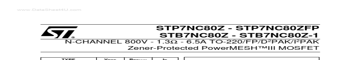
The third generation of MESH OVERLAY™ Power MOSFETs for very high voltage exhibits unsurpassed on-resistance per unit area while integrating back-to-back Zener diodes between gate and source. Such arrangement gives extra ESD capability with higher ruggedness performance as requested by a large variety of single-switch applications. INTERNAL SCHEMATIC DIAGRA.
OF GATE-TO-SOURCE ZENER DIODES The built-in back-to-back Zener diodes have specifically been designed to enhance not only the device’s ESD capability, but also to make them safely absorb possible voltage transients that may occasionally be applied from gate to source. In this respect the Zener voltage is appropriate to achieve an efficient and cost-effective intervention to protect the device’s integrity. These integrated Zener diodes thus avoid the usage of external components. 2/13 STP7NC80Z - STP7NC80ZFP - STB7NC80Z - STB7NC80Z-1 ELECTRICAL CHARACTERISTICS (TCASE =25°C UNLESS OTHERWISE SPE.
| No. | Partie # | Fabricant | Description | Fiche Technique |
|---|---|---|---|---|
| 1 | P7NC70ZF |

STMicroelectronics |
STP7NC70ZF |

|
| 2 | P7N06 |

Motorola Semiconductor |
MTP7N06 |
|
| 3 | P7N60B |

Intersil Corporation |
HGTP7N60B |
|
| 4 | P7N80 |

Fairchild Semiconductor |
FQP7N80 |
|
| 5 | P7N80C |
Fairchild Semiconductor |
FQP7N80C |
|
| 6 | P7NA40 |

ST Microelectronics |
STP7NA40 |
|
| 7 | P7NA60 |
STMicroelectronics |
N-Channel MOSFET |
|
| 8 | P7NA60FI |
STMicroelectronics |
N-Channel MOSFET |
|
| 9 | P7NB60 |
ST Microelectronics |
STP7NB60FP |
|
| 10 | P7NB60FP |
ST Microelectronics |
STP7NB60FP |
|
| 11 | P7NB80FP |
ST Microelectronics |
STP7NB80 |
|
| 12 | P7NK30Z |
STMicroelectronics |
STP7NK30Z |
|