
Recherchez avec le numéro de pièce ainsi que le fabricant ou la description
PIN # PIN NAME 1 PCI0/CR#_A 2 VDDPCI 3 PCI1/CR#_B 4 PCI2/TME 5 PCI3 6 PCI4/SRC5_EN 7 PCI_F5/ITP_EN 8 GNDPCI 9 VDD48 10 USB_48MHz/FSLA 11 GND48 12 VDD96_IO 13 DOTT_96/SRCT0 14 DOTC_96/SRCC0 15 GND 16 VDD TYPE I/O PWR I/O I/O OUT I/O I/O PWR PWR I/O PWR PWR OUT OUT PWR PWR DESCRIPTION 3.3V PCI clock output or Clock Request control A for either SRC0 or .
• 2 - CPU differential low power push-pull pairs
• 10 - SRC differential low power push-pull pairs
• 1 - CPU/SRC selectable differential low power push-pull
pair
• 1 - SRC/DOT selectable differential low power push-pull
pair
• 5 - PCI, 33MHz
• 1 - PCI_F, 33MHz free running
• 1 - USB, 48MHz
• 1 - REF, 14.318MHz
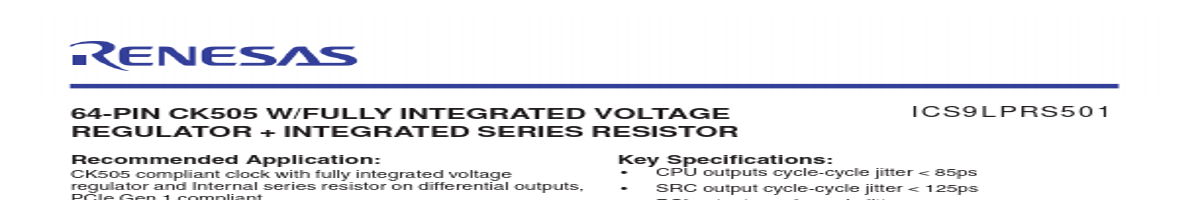
Key Specifications:
• CPU outputs cycle-cycle jitter < 85ps
• SRC output cycle-cycle jitter < 125ps
• PCI outputs cycle-cycle jitter < 250ps
• +/- 100ppm frequency accuracy on CPU & SRC
clocks
Features/Benefits:
• Does not require external pass transistor for voltage regulator
• Integr.

PIN # PIN NAME TYPE DESCRIPTION 3.3V PCI clock output or Clock Request control A for either SRC0 or SRC2 pair The power-.
| No. | Partie # | Fabricant | Description | Fiche Technique |
|---|---|---|---|---|
| 1 | ICS9LPRS502 |

IDT |
56-PIN CK505 W/FULLY INTEGRATED VOLTAGE REGULATOR + INTEGRATED SERIES RESISTOR |

|
| 2 | ICS9LPRS525 |

Integrated Device Technology |
56-pin CK505 |
|
| 3 | ICS9LPRS525 |

Renesas |
56-pin CK505 |
|
| 4 | ICS9LPRS535 |
Renesas |
VREG |
|
| 5 | ICS9LPRS535 |
Integrated Device Technology |
48-pin CK505 |
|
| 6 | ICS9LPRS545 |

Integrated Circuit Solution |
48-pin CK505 |
|
| 7 | ICS9LPRS365 |

ICS |
64-Pin CK505 w/Fully Integrated Voltage Regulator + Integrated Series Resistor |
|
| 8 | ICS9LPRS436C |
Integrated Device Technology |
Low Power Clock |
|
| 9 | ICS9LPRS462 |
Integrated Device Technology |
Low Power Clock |
|
| 10 | ICS9LPRS464 |
Integrated Device Technology |
System Clock Chip |
|
| 11 | ICS9LPRS480 |
Integrated Device Technology |
Programmable System Clock |
|
| 12 | ICS9LPR426A |

Integrated Circuit Systems |
Low Power Programmable Timing Control Hub |
|