
Recherchez avec le numéro de pièce ainsi que le fabricant ou la description
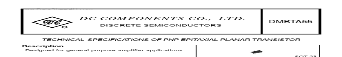
Designed for general purpose amplifier applications. SOT-23 Pinning 1 = Base 2 = Emitter 3 = Collector 1 .020(0.50) .012(0.30) 3 .063(1.60) .055(1.40) .108(0.65) .089(0.25) 2 Absolute Maximum Ratings(TA=25oC) Characteristic Collector-Base Voltage Collector-Emitter Voltage Emitter-Base Voltage Collector Current Total Power Dissipation Junction Temperatur.
ge Collector Cutoff Current Collector-Emitter Saturation Voltage(1) Base-Emitter On Voltage DC Current Gain(1) Transition Frequency (1)Pulse Test: Pulse Width (Ratings at 25 C ambient temperature unless otherwise specified) Symbol BVCBO BVCEO BVEBO ICBO ICEO VCE(sat) VBE(on) hFE1 hFE2 fT 380µs, Duty Cycle Min -60 -60 -4 80 80 50 2% Typ - Max -100 -100 -0.25 -1.2 250 - Unit V V V nA nA V V MHz Test Conditions IC=-100µA IC=-1mA IE=-100µA VCB=-60V VCE=-50V IC=-100mA, IB=-10mA IC=-100mA, VCE=-1V IC=-10mA, VCE=-1V IC=-100mA, VCE=-1V IC=-100mA, VCE=-1V .
| No. | Partie # | Fabricant | Description | Fiche Technique |
|---|---|---|---|---|
| 1 | DMBTA56 |

Dc Components |
NPN Transistor |

|
| 2 | DMBTA05 |
Dc Components |
NPN Transistor |
|
| 3 | DMBTA06 |
Dc Components |
NPN Transistor |
|
| 4 | DMBTA13 |
Dc Components |
NPN Transistor |
|
| 5 | DMBTA14 |
Dc Components |
NPN Transistor |
|
| 6 | DMBTA42 |
Dc Components |
NPN Transistor |
|
| 7 | DMBTA43 |
Dc Components |
NPN Transistor |
|
| 8 | DMBTA44 |
Dc Components |
NPN Transistor |
|
| 9 | DMBTA64 |
Dc Components |
NPN Transistor |
|
| 10 | DMBTA92 |
Dc Components |
NPN Transistor |
|
| 11 | DMBT1015 |
Dc Components |
PNP Transistor |
|
| 12 | DMBT1815 |
Dc Components |
PNP Transistor |
|