
Recherchez avec le numéro de pièce ainsi que le fabricant ou la description
Ball No. B2 C3 D3 D1 A1 A2 A3 A4 C2 C1 D2 D4 C4 B1 B4 B3 PIN Name DATA CLK VBAT1 PVCC PBAT LX PGND FB NRST OUT1 OUT2 OUT3 REFC VIO GND ADRS 6173 2.05±0.05 0.1±0.05 2.05±0.05 0.55MAX S P=0.5×3 0.275±0.05 B 4 S 0.06 16-φ0.25±0.05 0.05 A B D C (φ0.15)INDEX POST B A 1 2 3 A 0.275±0.05 P=0.5×3 Unit (mm) ● Block Diagram VBAT1 VIO DATA CLK ADRS NRST ww.
0mm×58mm. To use at temperature higher than 25C , derate 1% per 1C. Recommended Operating Conditions (Ta=25C) Parameter VBAT, PBAT Voltage Symbol
www.DataSheet.co.kr
V V V V mW ℃ ℃
Range
*
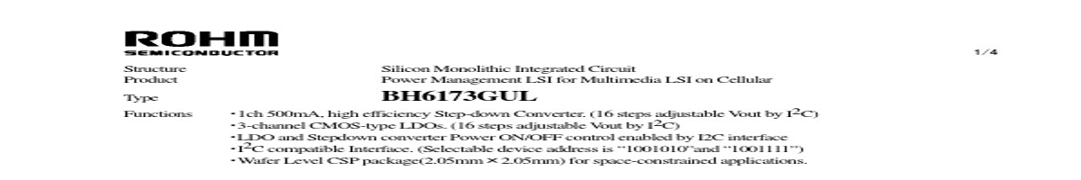
2 3
Unit V V
VBAT
2.20 ~ 5.20
VIO Voltage VIO
* 1.70 ~ 4.20
*2 Whenever the VBAT, PVCC and PBAT voltage is under the LDO, SWREG output voltage, the LDO and SWREG output is not guaranteed to meet its published specifications.
*3 The VIO Voltage must be under the Battery Voltage VBAT, PBAT at any times.
*This product is not especially designed to be protected from radioactivity.
REV. B
Datasheet pdf.
| No. | Partie # | Fabricant | Description | Fiche Technique |
|---|---|---|---|---|
| 1 | BH6172GU |

Rohm |
System Regulator |

|
| 2 | BH6176GU |
Rohm |
Silicon Monolithic Integrated Circuit |
|
| 3 | BH6111FV |
Rohm |
Power-unit |
|
| 4 | BH6113FV |
Rohm |
Power-unit |
|
| 5 | BH6114FV |
Rohm |
Power-unit |
|
| 6 | BH6150F |
Rohm |
System reset |
|
| 7 | BH616UV1610 |

Brilliance Semiconductor |
Ultra Low Power/High Speed CMOS SRAM |
|
| 8 | BH616UV1611 |
Brilliance Semiconductor |
Ultra Low Power/High Speed CMOS SRAM |
|
| 9 | BH616UV4010 |
Brilliance Semiconductor |
Ultra Low Power/High Speed CMOS SRAM 256K X 16 bit |
|
| 10 | BH616UV8010 |
Brilliance Semiconductor |
Ultra Low Power/High Speed CMOS SRAM |
|
| 11 | BH616UV8011 |
Brilliance Semiconductor |
Ultra Low Power/High Speed CMOS SRAM |
|
| 12 | BH6038KN |
Rohm |
Power Management |
|