
Recherchez avec le numéro de pièce ainsi que le fabricant ou la description
The MPC93R51 utilizes PLL technology to frequency and phase lock its outputs onto an input reference clock. Normal operation of the MPC93R51 requires a connection of one of the device outputs to the EXT_FB input to close the PLL feedback path. The reference clock frequency and the output divider for the feedback path determine the VCO frequency. Both must be.
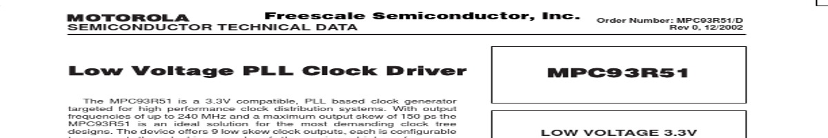
W Application Information The fully integrated PLL of the MPC93R51 allows the low skew outputs to lock onto a clock input and distribute it with essentially zero propagation delay to multiple components on the board. In zero-delay buffer mode, the PLL minimizes phase offset between the outputs and the reference signal. © Motorola, Inc. 2002 For More Information On This Product, 1 Go to: www.freescale.com Freescale Semiconductor, Inc. MPC93R51 PCLK PCLK TCLK REF_SEL EXT_FB (pullup) 0 Ref (pulldown) 1 0 PLL 1 ÷2 ÷4 ÷8 0 D 1 Q QA (pulldown) (pulldown) FB 200 - 480 MHz 0 D 1 (pullup) Q.
| No. | Partie # | Fabricant | Description | Fiche Technique |
|---|---|---|---|---|
| 1 | MPC93R52 |

Motorola |
LOW VOLTAGE 3.3V LVCMOS 1:11 CLOCK GENERATOR |

|
| 2 | MPC930 |
Motorola |
(MPC930 / MPC931) LOW VOLTAGE PLL CLOCK DRIVER |
|
| 3 | MPC931 |
Motorola |
(MPC930 / MPC931) LOW VOLTAGE PLL CLOCK DRIVER |
|
| 4 | MPC9315 |
Motorola |
2.5V and 3.3V CMOS PLL Clock Generator/Driver |
|
| 5 | MPC932 |
Motorola |
LOW VOLTAGE PLL CLOCK DRIVER |
|
| 6 | MPC9330 |
Motorola |
3.3V / 2.5V 1:6 LVCMOS PLL CLOCK GENERATOR |
|
| 7 | MPC9331 |
Motorola |
3.3 V 1:6 LVCMOS PLL Clock Generator |
|
| 8 | MPC9350 |
Motorola |
LOW VOLTAGE PLL CLOCK DRIVER |
|
| 9 | MPC9352 |
Motorola |
3.3V / 2.5V 1:11 LVCMOS ZERO DELAY CLOCK GENERATOR |
|
| 10 | MPC9352 |

IDT |
3.3V/2.5V 1:11 LVCMOS Zero Delay Clock Generator |
|
| 11 | MPC9100 |
Motorola |
DUAL PLL CLOCK GENERATOR |
|
| 12 | MPC9108 |
Motorola |
MULTIPLE OUTPUT CLOCK SYNTHESIZER |
|