
Recherchez avec le numéro de pièce ainsi que le fabricant ou la description
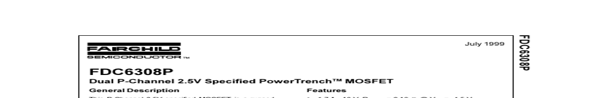
This P-Channel 2.5V specified MOSFET is a rugged gate version of Fairchild Semiconductor's advanced PowerTrench process. It has been optimized for power management applications with a wide range of gate drive voltage (2.5V - 12V). These devices have been designed to offer exceptional power dissipation in a very small footprint for applications where the bigg.
-1.7 A, -18 V. RDS(ON) = 0.18 Ω @ VGS = -4.5 V RDS(ON) = 0.30 Ω @ VGS = -2.5 V Extended VGSS range (±12V) for battery applications. Low gate charge (3nC typical). Fast switching speed. High performance trench technology for extremely low RDS(ON). Applications Load switch Battery protection Power management D2 S1 D1 SuperSOTTM-6 package: small footprint (72% smaller than standard SO-8); low profile (1mm thick). 4 3 5 2 G2 SuperSOT TM -6 S2 G1 TA = 25°C unless otherwise noted 6 1 Absolute Maximum Ratings Symbol VDSS VGSS ID PD Drain-Source Voltage Gate-Source .
| No. | Partie # | Fabricant | Description | Fiche Technique |
|---|---|---|---|---|
| 1 | FDC6301N |

Fairchild Semiconductor |
Dual N-Channel / Digital FET |

|
| 2 | FDC6301N |

ON Semiconductor |
Dual N-Channel Digital FET |
|
| 3 | FDC6302P |
Fairchild Semiconductor |
Digital FET/ Dual P-Channel |
|
| 4 | FDC6302P |
ON Semiconductor |
Dual P-Channel MOSFET |
|
| 5 | FDC6303N |
Fairchild Semiconductor |
Dual N-Channel Digital FET |
|
| 6 | FDC6304P |
Fairchild Semiconductor |
Digital FET/ Dual P-Channel |
|
| 7 | FDC6304P |
ON Semiconductor |
Dual P-Channel MOSFET |
|
| 8 | FDC6305N |
Fairchild Semiconductor |
Dual N-Channel MOSFET |
|
| 9 | FDC6305N |
ON Semiconductor |
Dual N-Channel MOSFET |
|
| 10 | FDC6306P |
Fairchild Semiconductor |
Dual P-Channel 2.5V Specified PowerTrench MOSFET |
|
| 11 | FDC6310P |
Fairchild Semiconductor |
Dual P-Channel 2.5V Specified PowerTrench MOSFET |
|
| 12 | FDC6310P |
ON Semiconductor |
Dual P-Channel MOSFET |
|