
Recherchez avec le numéro de pièce ainsi que le fabricant ou la description
The CDCVF310 is a high-performance, low-skew clock buffer that operates up to 200 MHz. Two banks of five outputs each provide low-skew copies of CLK. After power up, the default state of the outputs is low regardless of the state of the control pins. For normal operation, the outputs of bank 1Y[0:4] or 2Y[0:4] can be placed in a low state when the control pi.
1
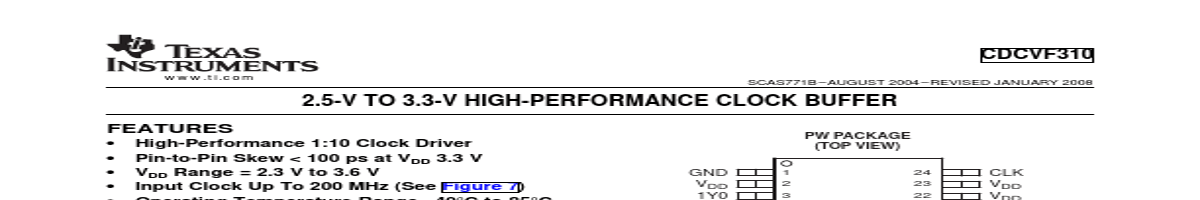
• High-Performance 1:10 Clock Driver
• Pin-to-Pin Skew < 100 ps at VDD 3.3 V
• VDD Range = 2.3 V to 3.6 V
• Input Clock Up To 200 MHz (See Figure 7)
• Operating Temperature Range
–40°C to 85°C
• Output Enable Glitch Suppression
• Distributes One Clock Input to Two Banks of
Five Outputs
• Packaged in 24-Pin TSSOP
• Pin-to-Pin Compatible to the CDCVF2310,
Except the R = 22-Ω Series Damping Resistors at Yn
APPLICATIONS
• General-Purpose Applications
GND VDD 1Y0 1Y1 1Y2 GND GND 1Y3 1Y4 VDD
1G 2Y4
PW PACKAGE (TOP VIEW)
1
24
2
23
3
22
4
21
5
20
6
19
7
18
8
17
9
16
10
15
11
.
| No. | Partie # | Fabricant | Description | Fiche Technique |
|---|---|---|---|---|
| 1 | CDCVF111 |

Texas Instruments |
1:9 DIFFERENTIAL LVPECL CLOCK DRIVER |

|
| 2 | CDCVF2310 |
Texas Instruments |
2.5-V to 3.3-V High-Performance Clock Buffer |
|
| 3 | CDCVF2310-EP |
Texas Instruments |
2.5-V TO 3.3-V HIGH-PERFORMANCE CLOCK BUFFER |
|
| 4 | CDCVF2505 |
Texas Instruments |
3.3-V Clock Phase-Lock Loop Clock Driver |
|
| 5 | CDCVF2505-Q1 |
Texas Instruments |
3.3-V CLOCK PHASE-LOCKED LOOP CLOCK DRIVER |
|
| 6 | CDCVF25081 |
Texas Instruments |
3.3-V Phased-Lock Loop Clock Driver |
|
| 7 | CDCVF25084 |
Texas Instruments |
3.3-V 1:8 ZERO DELAY x4 CLOCK MULTIPLIER |
|
| 8 | CDCVF2509 |
Texas Instruments |
3.3-V PHASE-LOCK LOOP CLOCK DRIVER |
|
| 9 | CDCVF2509A |
Texas Instruments |
3.3-V PHASE-LOCK LOOP CLOCK DRIVER |
|
| 10 | CDCVF2510 |
Texas Instruments |
3.3-V PHASE-LOCK LOOP CLOCK DRIVER |
|
| 11 | CDCVF2510A |
Texas Instruments |
3.3-V PHASE-LOCK LOOP CLOCK DRIVER |
|
| 12 | CDCVF855 |
Texas Instruments |
2.5-V PHASE-LOCKED-LOOP CLOCK DRIVER |
|