
Recherchez avec le numéro de pièce ainsi que le fabricant ou la description
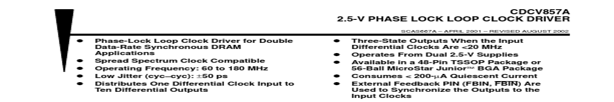
The CDCV857A is a high-performance, low-skew, low-jitter zero delay buffer that distributes a differential clock input pair (CLK, CLK) to ten differential pairs of clock outputs (Y[0:9], Y[0:9]) and one differential pair of feedback clock output (FBOUT, FBOUT). The clock outputs are controlled by the clock inputs (CLK, CLK), the feedback clocks (FBIN, FBIN),.
the feedback clocks (FBIN, FBIN), and the analog power input (AVDD). When PWRDWN is high, the outputs switch in phase and frequency with CLK. When PWRDWN is low, all outputs are disabled to high impedance state (3-state), and the PLL is shut down (low power mode). The device also enters this low power mode when the input frequency falls below a suggested detection frequency that is below 20 MHz (typical 10 MHz). An input frequency detection circuit will detect the low frequency condition and after applying a >20 MHz input signal this detection circuit turns on the PLL again and enables the ou.
| No. | Partie # | Fabricant | Description | Fiche Technique |
|---|---|---|---|---|
| 1 | CDCV857B |

Texas Instruments |
2.5-V PHASE LOCK LOOP CLOCK DRIVER |

|
| 2 | CDCV857BI |
Texas Instruments |
2.5-V PHASE LOCK LOOP CLOCK DRIVER |
|
| 3 | CDCV850 |
Texas Instruments |
2.5-V Phase Lock Loop Clock Driver |
|
| 4 | CDCV850I |
Texas Instruments |
2.5-V Phase Lock Loop Clock Driver |
|
| 5 | CDCV855 |
Texas Instruments |
2.5-V PHASE-LOCK LOOP CLOCK DRIVER |
|
| 6 | CDCV855I |
Texas Instruments |
2.5-V PHASE-LOCK LOOP CLOCK DRIVER |
|
| 7 | CDCV304 |
Texas Instruments |
200-MHz General-Purpose Clock Buffer |
|
| 8 | CDCV304-EP |
Texas Instruments |
General-Purpose Clock Buffer |
|
| 9 | CDCVF111 |
Texas Instruments |
1:9 DIFFERENTIAL LVPECL CLOCK DRIVER |
|
| 10 | CDCVF2310 |
Texas Instruments |
2.5-V to 3.3-V High-Performance Clock Buffer |
|
| 11 | CDCVF2310-EP |
Texas Instruments |
2.5-V TO 3.3-V HIGH-PERFORMANCE CLOCK BUFFER |
|
| 12 | CDCVF2505 |
Texas Instruments |
3.3-V Clock Phase-Lock Loop Clock Driver |
|