
Recherchez avec le numéro de pièce ainsi que le fabricant ou la description
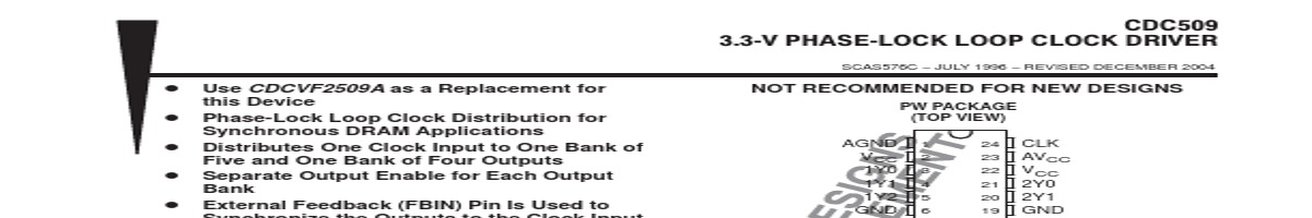
NOT RECOMMENDED FOR NEW DESIGNS PW PACKAGE (TOP VIEW) AGND 1 VCC 2 1Y0 3 1Y1 4 1Y2 5 GND 6 GND 7 1Y3 8 1Y4 9 VCC 10 1G 11 FBOUT 12 24 CLK 23 AVCC 22 VCC 21 2Y0 20 2Y1 19 GND 18 GND 17 2Y2 16 2Y3 15 VCC 14 2G 13 FBIN The CDC509 is a high-performance, low-skew, low-jitter, phase-lock loop (PLL) clock driver. It uses a PLL to precisely align, in both freque.
ifically designed for use with synchronous DRAMs. The CDC509 operates at 3.3-V VCC and is designed to drive up to five clock loads per output. One bank of five outputs and one bank of four outputs provide nine low-skew, low-jitter copies of CLK. Output signal duty cycles are adjusted to 50 percent, independent of the duty cycle at CLK. Each bank of outputs can be enabled or disabled separately via the control (1G and 2G) inputs. When the G inputs are high, the outputs switch in phase and frequency with CLK; when the G inputs are low, the outputs are disabled to the logic-low state. Unlike many.
| No. | Partie # | Fabricant | Description | Fiche Technique |
|---|---|---|---|---|
| 1 | CDC516 |

Texas Instruments |
3.3-V Phase-Lock-Loop Clock Driver |

|
| 2 | CDC536 |
Texas Instruments |
3.3-V Phase-Lock-Loop Clock Driver |
|
| 3 | CDC5801A |
Texas Instruments |
Low Jitter Clock Multiplier/Divider |
|
| 4 | CDC5806 |
Texas Instruments |
THREE PLLs BASED CLOCK GENERATOR |
|
| 5 | CDC582 |
Texas Instruments |
3.3-V Phase-Lock-Loop Clock Driver |
|
| 6 | CDC586 |
Texas Instruments |
3.3-V Phase-Lock-Loop Clock Driver |
|
| 7 | CDC5D23B |

Sumida Corporation |
(CDC4D20 / CDC5D23B) POWER INDUCTORS |
|
| 8 | CDC-Z137 |

Aiwa |
FM / AM CD Player |
|
| 9 | CDC1104 |
Texas Instruments |
1 to 4 Configurable Clock Buffer |
|
| 10 | CDC111 |
Texas Instruments |
1-LINE TO 9-LINE DIFFERENTIAL LVPECL CLOCK DRIVER |
|
| 11 | CDC1607F-E |

Micronas |
Automotive Controller Specification |
|
| 12 | CDC1631F-E |
Micronas |
Automotive Controller |
|