
Recherchez avec le numéro de pièce ainsi que le fabricant ou la description
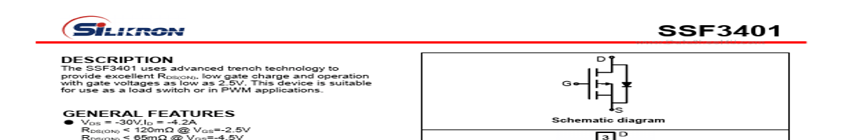
The SSF3401 uses advanced trench technology to provide excellent RDS(ON), low gate charge and operation with gate voltages as low as 2.5V. This device is suitable for use as a load switch or in PWM applications. D G GENERAL FEATURES ● VDS = -30V,ID = -4.2A RDS(ON) < 120mΩ @ VGS=-2.5V RDS(ON) < 65mΩ @ VGS=-4.5V RDS(ON) < 50mΩ @ VGS=-10V ● High Power and cu.
● VDS = -30V,ID = -4.2A RDS(ON) < 120mΩ @ VGS=-2.5V RDS(ON) < 65mΩ @ VGS=-4.5V RDS(ON) < 50mΩ @ VGS=-10V
● High Power and current handing capability
● Lead free product is acquired
● Surface Mount Package
S
Schematic diagram
Marking and pin Assignment
Application
●PWM applications
●Load switch
●Power management SOT-23 top view
PACKAGE MARKING AND ORDERING INFORMATION Device Marking Device Device Package Reel Size
3401 SSF3401 SOT-23 Ø180mm
Tape width
8 mm
Quantity
3000 units
ABSOLUTE MAXIMUM RATINGS(TA=25℃unless otherwise noted) Parameter Symbol
Drain-Source Voltage Gate-Source Voltage .
| No. | Partie # | Fabricant | Description | Fiche Technique |
|---|---|---|---|---|
| 1 | SSF3400K |

Silikron |
MOSFET |

|
| 2 | SSF3402 |

Silikron Semiconductor Co |
MOSFET |
|
| 3 | SSF3415 |

GOOD-ARK |
20V P-Channel MOSFET |
|
| 4 | SSF3416 |

Silikron Semiconductor |
MOSFET |
|
| 5 | SSF3420 |
Silikron Semiconductor Co |
PWM applications |
|
| 6 | SSF3420 |
GOOD-ARK |
N-Channel MOSFET |
|
| 7 | SSF3428 |
Silikron Semiconductor Co |
PWM applications |
|
| 8 | SSF3428 |
GOOD-ARK |
N-Channel MOSFET |
|
| 9 | SSF3002EG1 |
Silikron |
MOSFET |
|
| 10 | SSF3006DB |
Silikron |
MOSFET |
|
| 11 | SSF3006DBC |
Silikron |
MOSFET |
|
| 12 | SSF3014 |
Silikron Semiconductor Co |
N-Channel MOSFET |
|