
Recherchez avec le numéro de pièce ainsi que le fabricant ou la description
It utilizes the latest processing techniques to achieve the high cell density and reduces the on-resistance with high repetitive avalanche rating. These features combine to make this design an extremely efficient and reliable device for use in power switching application and a wide variety of other applications. Absolute Max Rating: Symbol ID @ TC = 25°C .
Advanced MOSFET process technology
Special designed for PWM, load switching and
general purpose applications
Ultra low on-resistance with low gate charge
Fast switching and reverse body recovery
150℃ operating temperature
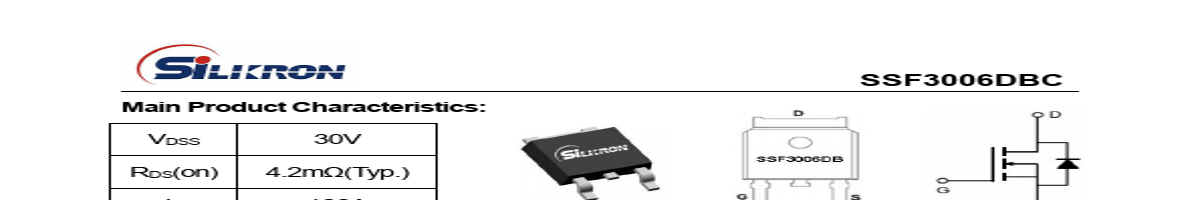
SSF3006DBC
Marking and Pin Assignments
Schematic Diagram
Description:
It utilizes the latest processing techniques to achieve the high cell density and reduces the on-resistance with high repetitive avalanche rating. These features combine to make this design an extremely efficient and reliable device for use in power switching application and a wide variety of.
| No. | Partie # | Fabricant | Description | Fiche Technique |
|---|---|---|---|---|
| 1 | SSF3006DB |

Silikron |
MOSFET |

|
| 2 | SSF3002EG1 |
Silikron |
MOSFET |
|
| 3 | SSF3014 |

Silikron Semiconductor Co |
N-Channel MOSFET |
|
| 4 | SSF3018 |
Silikron Semiconductor Co |
N-Channel MOSFET |
|
| 5 | SSF3018D |
Silikron Semiconductor Co |
N-Channel MOSFET |
|
| 6 | SSF3022 |
Silikron Semiconductor Co |
N-Channel MOSFET |
|
| 7 | SSF3022D |
Silikron Semiconductor Co |
N-Channel MOSFET |
|
| 8 | SSF3028C1 |
Silikron |
MOSFET |
|
| 9 | SSF3035L |
Silikron |
MOSFET |
|
| 10 | SSF3036C |

GOOD-ARK |
30V Complementary MOSFET |
|
| 11 | SSF3036C |

Silikron Semiconductor |
MOSFET |
|
| 12 | SSF3051G7 |
Silikron Semiconductor |
MOSFET |
|