
Recherchez avec le numéro de pièce ainsi que le fabricant ou la description
The SSF3314E uses advanced trench technology to provide excellent RDS(ON), low gate charge and operation with gate voltages as low as 2.5V while retaining a 12V VGS(MAX) rating. It is ESD protected. This device is suitable for use as a uni-directional or bi-directional load switch, facilitated by its common-drain configuration. GENERAL FEATURES ● VDS = 30V,I.
● VDS = 30V,ID = 8A RDS(ON) < 39mΩ @ VGS=2.5V RDS(ON) < 28mΩ @ VGS=3.1V RDS(ON) < 24mΩ @ VGS=4.0V RDS(ON) < 23mΩ @ VGS=4.5V RDS(ON) < 18mΩ @ VGS=10V
ESD Rating:2000V HBM
● High Power and current handing capability
● Lead free product
● Surface Mount Package
SSF3314E
30V N-Channel MOSFET
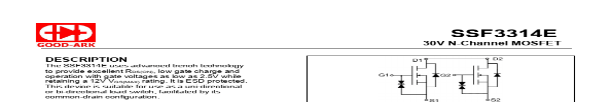
Schematic Diagram Pin Assignment DFN3×3-8L Bottom View
PACKAGE MARKING AND ORDERING INFORMATION
Device Marking
Device
Device Package
Reel Size
SSF3314E
SSF3314E
DFN3×3-8L
-
Tape Width -
Quantity -
ABSOLUTE MAXIMUM RATINGS (TA=25℃unless otherwise noted)
Parameter
Symbol
Drain-Source Voltage
VDS
.

The SSF3314E uses advanced trench technology to provide excellent RDS(ON), low gate charge and operation with gate volta.
| No. | Partie # | Fabricant | Description | Fiche Technique |
|---|---|---|---|---|
| 1 | SSF3322 |

Silikron Semiconductor |
MOSFET |

|
| 2 | SSF3324 |

Silikron Semiconductor Co |
MOSFET |
|
| 3 | SSF3324 |

GOOD-ARK |
N-Channel MOSFET |
|
| 4 | SSF3338 |

Silikron Semiconductor Co |
MOSFET |
|
| 5 | SSF3338 |
GOOD-ARK |
N-Channel MOSFET |
|
| 6 | SSF3339 |
Silikron Semiconductor |
MOSFET |
|
| 7 | SSF3339 |
GOOD-ARK |
P-Channel MOSFET |
|
| 8 | SSF3341 |
Silikron Semiconductor |
MOSFET |
|
| 9 | SSF3341 |
GOOD-ARK |
P-Channel MOSFET |
|
| 10 | SSF3341L |
Silikron Semiconductor |
MOSFET |
|
| 11 | SSF3341L |
GOOD-ARK |
P-Channel MOSFET |
|
| 12 | SSF3341UP |

Silikron |
MOSFET |
|