
Recherchez avec le numéro de pièce ainsi que le fabricant ou la description
and charts stated herein. Infineon Technologies is an approved CECC manufacturer. Information For further information on technology, delivery terms and conditions and prices please contact your nearest Infineon Technologies Office in Germany or our Infineon Technologies Reprensatives worldwide (see address list). Warnings Due to technical requirements compo.
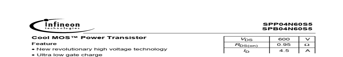
ture Rev. 2.1 Page 1 2004-03-30 SPP04N60S5 SPB04N60S5 Maximum Ratings Parameter Drain Source voltage slope V DS = 480 V, ID = 4.5 A, Tj = 125 °C Symbol dv/dt Value 20 Unit V/ns Thermal Characteristics Parameter Thermal resistance, junction - case Thermal resistance, junction - ambient, leaded SMD version, device on PCB: @ min. footprint @ 6 cm2 cooling area 2) Soldering temperature, 1.6 mm (0.063 in.) from case for 10s 3) Electrical Characteristics, at Tj=25°C unless otherwise specified Parameter Symbol Conditions min. Drain-source breakdown voltage V(BR)DSS VGS=0V, ID=0.25mA Drain-Sou.

Isc N-Channel MOSFET Transistor SPB04N60S5 ·FEATURES ·With To-263(D2PAK) package ·Low input capacitance and gate charg.
| No. | Partie # | Fabricant | Description | Fiche Technique |
|---|---|---|---|---|
| 1 | SPB04N60C2 |

Infineon |
Cool MOS Power Transistor |

|
| 2 | SPB04N60C2 |

Infineon Technologies |
Cool MOS Power Transistor |
|
| 3 | SPB04N60C3 |
Infineon Technologies |
Cool MOS Power Transistor |
|
| 4 | SPB04N60C3 |

INCHANGE |
N-Channel MOSFET |
|
| 5 | SPB04N50C3 |
INCHANGE |
N-Channel MOSFET |
|
| 6 | SPB04N50C3 |
Infineon Technologies |
Power Transistor |
|
| 7 | SPB02N60C3 |
Infineon Technologies |
Cool MOS Power Transistor |
|
| 8 | SPB02N60C3 |
INCHANGE |
N-Channel MOSFET |
|
| 9 | SPB02N60S5 |
Infineon Technologies |
Cool MOS Power Transistor |
|
| 10 | SPB02N60S5 |
INCHANGE |
N-Channel MOSFET |
|
| 11 | SPB03N60C3 |
Infineon Technologies |
Cool MOS& Power Transistor |
|
| 12 | SPB03N60C3 |
INCHANGE |
N-Channel MOSFET |
|