
Recherchez avec le numéro de pièce ainsi que le fabricant ou la description
of each pin can be found in the Functional Pin Description section beginning on page 20. Pin 1 2 3 4 5 6, 33, 49, 50, 52, 53 7 8 9 10 11 Pin Name PHASEA PGND EN1 EN2 RST N/C PUMP VPUMP VBAT PHASEB PHASEC Pin Function Digital Output Ground Digital Input Digital Input Digital Input – Power Drive Out Power Input Digital Input Digital Output Digital Output Forma.
• Fully specified from 8.0V to 40V covers 12V and 24V automotive systems
• Extended operating range from 6.0V to 58V covers 12V and 42V systems
• 1.0A gate drive capability with protection
• Protection against reverse charge injection from CGD and CGS of external FETs
• Includes a charge pump to support full FET drive at low battery voltages
• Deadtime is programmable via the SPI port
• Simultaneous output capability enabled via safe SPI command
• Pb-Free Packaging Designated by Suffix Code EK
VBAT
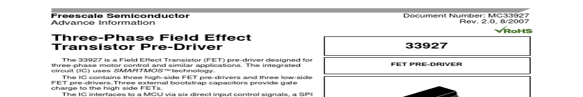
33927
FET PRE-DRIVER
EK SUFFIX (Pb-FREE) 98ASA99334D 54-PIN SOICW-EP
ORDERING INFORMATION
Dev.
| No. | Partie # | Fabricant | Description | Fiche Technique |
|---|---|---|---|---|
| 1 | MC3392 |

Motorola |
LOW SIDE PROTECTED SWITCH |

|
| 2 | MC33926 |

Freescale Semiconductor |
5.0A Throttle Control H-Bridge |
|
| 3 | MC33926 |

NXP |
5.0A throttle control H-bridge |
|
| 4 | MC33901 |
Freescale Semiconductor |
High-speed CAN Transceiver |
|
| 5 | MC33902 |
Motorola |
High Speed CAN Interface |
|
| 6 | MC33903 |
NXP |
SBC Gen2 |
|
| 7 | MC33904 |
NXP |
SBC Gen2 |
|
| 8 | MC33905 |
NXP |
SBC Gen2 |
|
| 9 | MC33907 |
NXP |
Power-system |
|
| 10 | MC33908 |
NXP |
Power-system |
|
| 11 | MC33910 |
NXP |
LIN transceiver |
|
| 12 | MC33911 |
NXP |
LIN transceiver |
|