
Recherchez avec le numéro de pièce ainsi que le fabricant ou la description
Pin Name K, K SAn DQn SW SWa SWb SWc SWd ZZ VDD Pin Description Differential Clocks Synchronous Address Input Bi-directional Data Bus Synchronous Global Write Enable Synchronous Byte a Write Enable Synchronous Byte b Write Enable Synchronous Byte c Write Enable Synchronous Byte d Write Enable Asynchronous Power Down Core Power Supply Pin Name VDDQ M1, M2 .
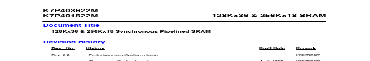
• 128Kx36 or 256Kx18 Organizations.
• 3.3V Core Power Supply.
• LVTTL Input and Output Levels.
• Differential, PECL Clock Inputs K, K.
• Synchronous Read and Write Operation
• Registered Input and Registered Output
• Internal Pipeline Latches to Support Late Write.
• Byte Write Capability(four byte write selects, one for each 9bits)
• Synchronous or Asynchronous Output Enable.
• Power Down Mode via ZZ Signal.
• JTAG 1149.1 Compatible Test Access port.
• 119(7x17)Pin Ball Grid Array Package(14mmx22mm)
Organization
Part Number
128Kx36 256Kx18
K7P403622M-H20 K7P403622M-H16 K7P403622M-H19 K7P4.
| No. | Partie # | Fabricant | Description | Fiche Technique |
|---|---|---|---|---|
| 1 | K7P403622B |

Samsung |
SRAM |

|
| 2 | K7P403623B |

Samsung semiconductor |
128Kx36 & 256Kx18 SRAM |
|
| 3 | K7P401822B |
Samsung |
SRAM |
|
| 4 | K7P401822M |
Samsung |
SRAM |
|
| 5 | K7P401823B |
Samsung semiconductor |
128Kx36 & 256Kx18 SRAM |
|
| 6 | K7P161866A |
Samsung semiconductor |
(K7P161866A / K7P163866A) 512Kx36 AND 1Mx18 Synchronous Pipelined SRAM |
|
| 7 | K7P163866A |
Samsung semiconductor |
(K7P161866A / K7P163866A) 512Kx36 AND 1Mx18 Synchronous Pipelined SRAM |
|
| 8 | K7P321866M |
Samsung semiconductor |
1Mx36 & 2Mx18 SRAM |
|
| 9 | K7P321874C |

Samsung Electronics |
1Mx36 & 2Mx18 SRAM |
|
| 10 | K7P321874C |
Samsung Electronics |
1Mx36 & 2Mx18 SRAM |
|
| 11 | K7P321888M |
Samsung Electronics |
1Mx36 & 2Mx18 SRAM |
|
| 12 | K7P321888M |
Samsung Electronics |
1Mx36 & 2Mx18 SRAM |
|