
Recherchez avec le numéro de pièce ainsi que le fabricant ou la description
TECHNICAL DATA IW4042B Quad Clocked «D» Latch High-Voltage Silicon-Gate CMOS IW4042B types contain four latch circuits, each strobed by a common clock. Complementary buffered outputs are available from each circuit. The impedance of the n- and p-channel output devices is balanced and all outputs are electrically identical. Information present at the data i.
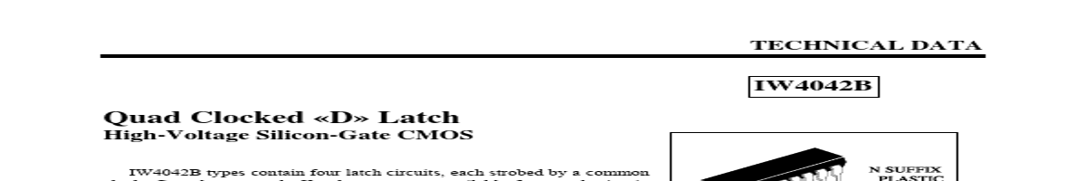
D and F suffixes); 16-lead dual-in-line plastic package (E suffix), and in chip form (H suffix).
• Operating Voltage Range: 3.0 to 18 V
• Maximum input current of 1 µA at 18 V over full packagetemperature range; 100 nA at 18 V and 25°C
• Noise margin (over full package temperature range): 1.0 V min @ 5.0 V supply 2.0 V min @ 10.0 V supply 2.5 V min @ 15.0 V supply
ORDERING INFORMATION IW4042BN Plastic IW4042BD SOIC TA = -55° to 125° C for all packages
PIN ASSIGNMENT
FUNCTION TABLE
Inputs Clock Polarity 0 0 1 1 Outputs Q D Latch D Latch
w
w
w
.d
e e h s a t a
. u t4
m o c
0 1 1 0
PI.
| No. | Partie # | Fabricant | Description | Fiche Technique |
|---|---|---|---|---|
| 1 | IW4040B |

IK Semiconductor |
12-Bit Binary Counter |

|
| 2 | IW4043B |
IK Semiconductor |
Quad NOR R-S Latch (3-State) |
|
| 3 | IW4049B |
IK Semiconductor |
Hex Buffer/Converter |
|
| 4 | IW4001B |
IK Semiconductor |
Quad 2-Input NOR Gate |
|
| 5 | IW4002B |
IK Semiconductor |
Dual 4-Input NOR Gate |
|
| 6 | IW4006B |
IK Semiconductor |
18-Bit Static Shift Register |
|
| 7 | IW4011B |
IK Semiconductor |
Quad 2-Input NAND Gate |
|
| 8 | IW4012B |
IK Semiconductor |
Dual 4-Input NAND Gate |
|
| 9 | IW4013B |

ETC |
Dual D Flip-Flop High-Voltage Silicon-Gate CMOS |
|
| 10 | IW4013B |
IK Semiconductor |
Dual D-Type Flip-Flop |
|
| 11 | IW4015B |
IK Semiconductor |
Dual 4-Bit Static Shift Register |
|
| 12 | IW4017B |
IK Semiconductor |
Decade Counter/Driver |
|