
Recherchez avec le numéro de pièce ainsi que le fabricant ou la description
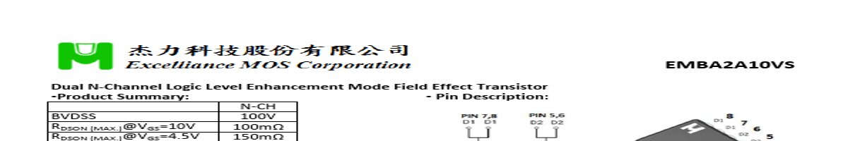
N-CH BVDSS 100V RDSON (MAX.)@VGS=10V RDSON (MAX.)@VGS=4.5V 100mΩ 150mΩ ID @TC=25℃ 9.0A ID @TA=25℃ 3.0A Dual N Channel MOSFET UIS、Rg 100% Tested Pb-Free Lead Plating & Halogen Free ▪ABSOLUTE MAXIMUM RATINGS (TC = 25 °C Unless Otherwise Noted) PARAMETERS/TEST CONDITIONS SYMBOL Gate-Source Voltage Continuous Drain Current Continuous Drain Curren.
1Pulse width limited by maximum junction temperature. 2Duty cycle < 1% 360°C / W when mounted on a 1 in2 pad of 2 oz copper. 4Guarantee by Engineering test TYPICAL 2021/3/15 A.0 MAXIMUM 9 60 UNIT °C/W P.1 EMBA2A10VS ▪ELECTRICAL CHARACTERISTICS (TJ = 25 °C, Unless Otherwise Noted) PARAMETER SYMBOL TEST CONDITIONS MIN STATIC Drain-Source Breakdown Voltage4 Gate Threshold Voltage4 Gate-Body Leakage4 Zero Gate Voltage Drain Current4 On-State Drain Current1 Drain-Source On-State Resistance1,4 Forward Transconductance1 V(BR)DSS VGS(th) IGSS IDSS ID(ON) RDS(ON) gfs VGS = 0V, ID = 250.
| No. | Partie # | Fabricant | Description | Fiche Technique |
|---|---|---|---|---|
| 1 | EMBA2A06HS |

Excelliance MOS |
Dual N-Channel Logic Level Enhancement Mode Field Effect Transistor |

|
| 2 | EMBA2N10A |
Excelliance MOS |
N-Channel Logic Level Enhancement Mode Field Effect Transistor |
|
| 3 | EMBA2N10AS |
Excelliance MOS |
N-Channel Logic Level Enhancement Mode Field Effect Transistor |
|
| 4 | EMBA0A10G |
Excelliance MOS |
MOSFET |
|
| 5 | EMBA0N10A |
Excelliance MOS |
N-Channel Logic Level Enhancement Mode Field Effect Transistor |
|
| 6 | EMBA0N10CS |
Excelliance MOS |
N-Channel Logic Level Enhancement Mode Field Effect Transistor |
|
| 7 | EMBA0N10F |
Excelliance MOS |
MOSFET |
|
| 8 | EMBA0N10G |
Excelliance MOS |
MOSFET |
|
| 9 | EMBA0N10S |
Excelliance MOS |
MOSFET |
|
| 10 | EMBA1N10A |
Excelliance MOS |
MOSFET |
|
| 11 | EMBA1N10Q |
Excelliance MOS |
N-Channel Logic Level Enhancement Mode Field Effect Transistor |
|
| 12 | EMBA3P03JS |
Excelliance MOS |
P-Channel Logic Level Enhancement Mode Field Effect Transistor |
|