
Recherchez avec le numéro de pièce ainsi que le fabricant ou la description
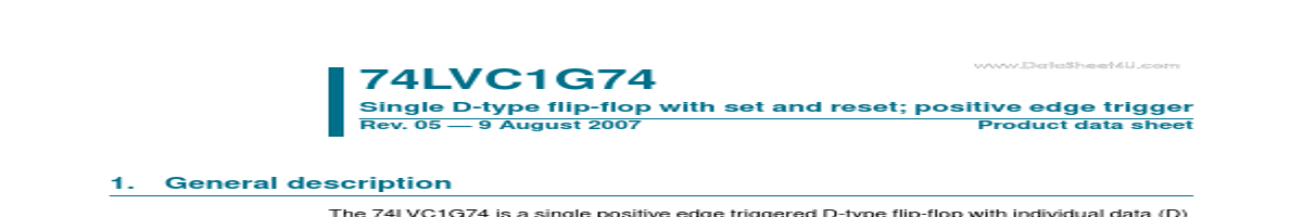
The 74LVC1G74 is a single positive edge triggered D-type flip-flop with individual data (D) inputs, clock (CP) inputs, set (SD) and (RD) inputs, and complementary Q and Q outputs. This device is fully specified for partial power-down applications using IOFF. The IOFF circuitry disables the output, preventing damaging backflow current through the device when it i.
s s s s Wide supply voltage range from 1.65 V to 5.5 V 5 V tolerant inputs for interfacing with 5 V logic High noise immunity Complies with JEDEC standard: x JESD8-7 (1.65 V to 1.95 V) x JESD8-5 (2.3 V to 2.7 V) x JESD8-B/JESD36 (2.7 V to 3.6 V) ±24 mA output drive (VCC = 3.0 V) ESD protection: x HBM EIA/JESD22-A114E exceeds 2000 V x MM EIA/JESD22-A115-A exceeds 200 V CMOS low power consumption Latch-up performance exceeds 250 mA Direct interface with TTL levels Inputs accept voltages up to 5 V Multiple package options Specified from −40 °C to +85 °C and −40 °C to +125 °C s s s s s s s s NXP.

The 74LVC1G74 is a single positive edge triggered D-type flip-flop with individual data (D), clock (CP), set (SD) and re.
| No. | Partie # | Fabricant | Description | Fiche Technique |
|---|---|---|---|---|
| 1 | 74LVC1G74-Q100 |

nexperia |
Single D-type flip-flop |

|
| 2 | 74LVC1G79 |
nexperia |
Single D-type flip-flop |
|
| 3 | 74LVC1G79 |

NXP Semiconductors |
Single D-type flip-flop positive-edge trigger |
|
| 4 | 74LVC1G79-Q100 |
nexperia |
Single D-type flip-flop |
|
| 5 | 74LVC1G00 |

Diodes |
SINGLE 2 INPUT POSITIVE NAND GATE |
|
| 6 | 74LVC1G00 |
nexperia |
Single 2-input NAND gate |
|
| 7 | 74LVC1G00-Q100 |
nexperia |
Single 2-input NAND gate |
|
| 8 | 74LVC1G02 |
Diodes |
SINGLE 2 INPUT POSITIVE NOR GATE |
|
| 9 | 74LVC1G02 |
nexperia |
Single 2-input NOR gate |
|
| 10 | 74LVC1G02-Q100 |
nexperia |
Single 2-input NOR gate |
|
| 11 | 74LVC1G04 |
nexperia |
Single inverter |
|
| 12 | 74LVC1G04 |
Diodes |
SINGLE INVERTER |
|