
Recherchez avec le numéro de pièce ainsi que le fabricant ou la description
It utilizes the advanced trench processing techniques to achieve extremely low on resistance and low gate charge. These features combine to make this design an extremely efficient and reliable device for use in PWM, load switching and a wide variety of other applications. Absolute Max Rating: Symbol ID @ TC = 25°C ID @ TC = 70°C IDM PD @TC = 25°C VDS VGS .
Advanced trench MOSFET process technology
Special designed for PWM, load switching and
general purpose applications
Ultra low on-resistance with low gate charge
High Power and current handing capability
Fully Avalanche Rated
ESD Protection HBM ≥ 2KV
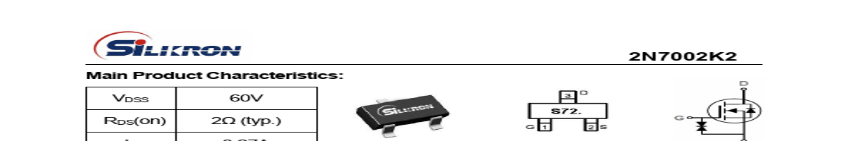
2N7002K2
Marking and pin Assignments
Schematic Diagram
Description:
It utilizes the advanced trench processing techniques to achieve extremely low on resistance and low gate charge. These features combine to make this design an extremely efficient and reliable device for use in PWM, load switching and a wide variety of other applic.
| No. | Partie # | Fabricant | Description | Fiche Technique |
|---|---|---|---|---|
| 1 | 2N7002K |

DIODES |
N-CHANNEL ENHANCEMENT MODE MOSFET |

|
| 2 | 2N7002K |

Kexin |
N-channel MOSFET |
|
| 3 | 2N7002K |

HOTTECH |
N-Channel MOSFET |
|
| 4 | 2N7002K |

MCC |
N-Channel MOSFET |
|
| 5 | 2N7002K |

WEITRON |
N-Channel Enhancement Mode Power MOSFET |
|
| 6 | 2N7002K |

Vishay Siliconix |
N-channel MOSFET |
|
| 7 | 2N7002K |

ON Semiconductor |
Small-Signal MOSFET |
|
| 8 | 2N7002K |

Fairchild Semiconductor |
N-channel MOSFET |
|
| 9 | 2N7002K |

Philips |
N-channel MOSFET |
|
| 10 | 2N7002K |

Pan Jit International |
N-channel MOSFET |
|
| 11 | 2N7002K |

SeCoS |
N-channel MOSFET |
|
| 12 | 2N7002K |

AUK |
N-channel MOSFET |
|