Recherchez avec le numéro de pièce ainsi que le fabricant ou la description
MC100LVEL39 |


| Part Number | MC100LVEL39 |
| Manufacturer | Motorola |
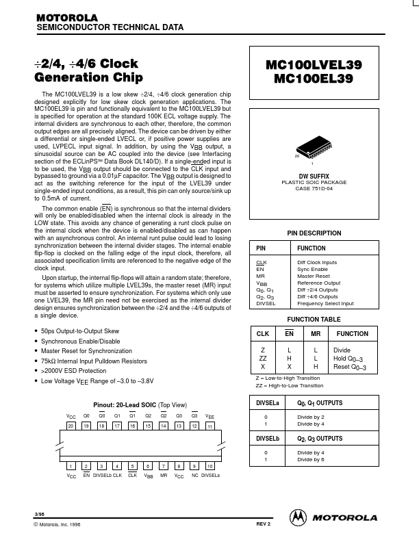
| Description | PIN CLK EN MR VBB Q0, Q1 Q2, Q3 DIVSEL FUNCTION Diff Clock Inputs Sync Enable Master Reset Reference Output Diff ÷2/4 Outputs Diff ÷4/6 Outputs Frequency Select Input FUNCTION TABLE CLK Z ZZ X EN L H... |
| Features |
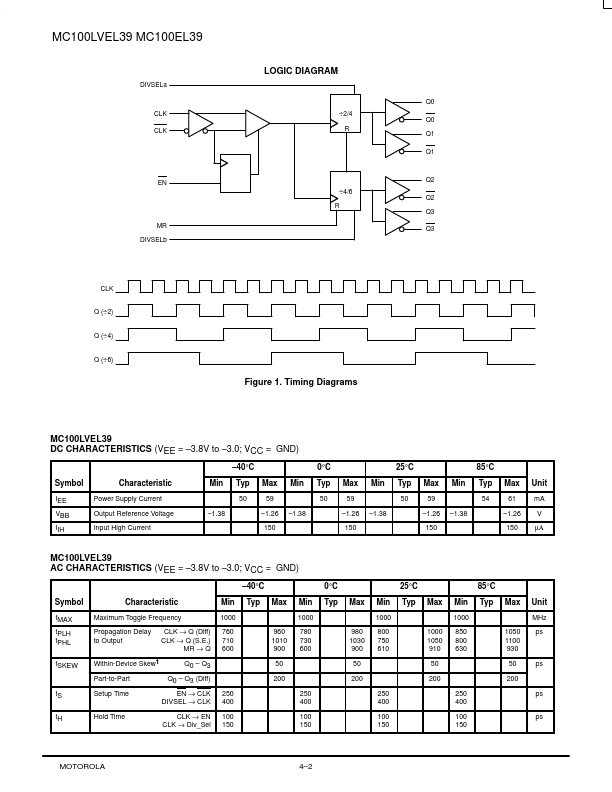
single-ended input conditions, as a result, this pin can only source/sink up to 0.5mA of current. The common enable (EN) is synchronous so that the internal dividers will only be enabled/disabled when the internal clock is already in the LOW state. This avoids any chance of generating a runt clock pulse on the internal clock when the device is enabled/disabled as can happen with an asynchronous control. An internal runt pulse could lead to losing synchronization between the internal divider stages. The internal enable flip-flop is clocked on the falling edge of the input clock, therefore, all ... |
| Document |
PDF 127.05KB |
| Distributor | Stock | Price | Buy |
|---|
| No. | Partie # | Fabricant | Description | Fiche Technique |
|---|---|---|---|---|
| 1 | MC100LVEL30 |

Motorola |
Triple D Flip-Flop |

|
| 2 | MC100LVEL30 |
ON Semiconductor |
Triple D Flip-Flop |

|
| 3 | MC100LVEL31 |

Motorola |
D Flip-Flop |

|
| 4 | MC100LVEL31 |
ON Semiconductor |
3.3V ECL D Flip?Flop |

|
| 5 | MC100LVEL32 |

Motorola |
Divider |

|