
Recherchez avec le numéro de pièce ainsi que le fabricant ou la description
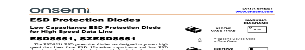
of survivability specs. MARKING DIAGRAMS X2DFN2 CASE 714AB AM A = Specific Device Code M = Date Code X2DFNW2 CASE 711BG KM K = Specific Device Code M = Date Code PIN CONFIGURATION AND SCHEMATIC 1 2 = ORDERING INFORMATION See detailed ordering and shipping information on page 2 of this data sheet. Semiconductor Components Industries, LLC, 2.
Low Capacitance (0.30 pF Max, I/O to GND)
Protection for the Following IEC Standards:
IEC 61000−4−2 (Level 4) & ISO 10605
Low ESD Clamping Voltage
SZESD8551MXWT5G − Wettable Flank Package for Optimal
Automated Optical Inspection (AOI)
SZ Prefix for Automotive and Other Applications Requiring Unique
Site and Control Change Requirements; AEC−Q101 Qualified and PPAP Capable
These Devices are Pb−Free, Halogen Free/BFR Free and are RoHS
Compliant
Typical Applications
USB 3.0
MHL 2.0
eSATA
MAXIMUM RATINGS (TJ = 25C unless otherwise noted)
Rating
Symbol
Value
Unit
Operating J.
| No. | Partie # | Fabricant | Description | Fiche Technique |
|---|---|---|---|---|
| 1 | SZESD8351 |

ON Semiconductor |
ESD Protection Diode |

|
| 2 | SZESD8351P2 |
ON Semiconductor |
ESD Protection Diode |
|
| 3 | SZESD8451 |
ON Semiconductor |
ESD Protection Diodes |
|
| 4 | SZESD1014 |
ON Semiconductor |
Low Capacitance ESD Protection Array |
|
| 5 | SZESD1L001 |
ON Semiconductor |
ESD Protection Diode |
|
| 6 | SZESD5B5.0S |
ON Semiconductor |
ESD Protection Diode |
|
| 7 | SZESD5Z2.5T1G |
ON Semiconductor |
ESD Protection Diode |
|
| 8 | SZESD7002 |
ON Semiconductor |
ESD Protection Diode |
|
| 9 | SZESD7004 |
ON Semiconductor |
SD Protection Diode |
|
| 10 | SZESD7008 |
ON Semiconductor |
ESD Protection Diodes |
|
| 11 | SZESD7016 |
ON Semiconductor |
ESD Protection Diode |
|
| 12 | SZESD7102 |
ON Semiconductor |
ESD Protection Diodes |
|