
Recherchez avec le numéro de pièce ainsi que le fabricant ou la description
PIN # PIN NAME 1 *FS0/REF0 2 VDDREF 3 X1 4 X2 5 GND 6 *(PCICLK7/HTTCLK0)ModeA 7 *PCICLK8/HTTCLK1/ModeB 8 PCICLK9/HTTCLK2 9 VDDPCI 10 GND 11 ~PCICLK10/HTTCLK3 12 PCICLK11 13 PCICLK0 14 PCICLK1 15 GND 16 VDDPCI 17 ****PCICLK2 18 ****PCICLK3 19 VDDPCI 20 GND 21 PCICLK4 22 PCICLK5 23 ~*PCICLK_F/ModeC 24 ~*(PCICLK6)PCI_STOP# 25 SCLK 26 SDATA 27 GND PIN TYPE .
• 2 - Differential pair push-pull CPU clocks @
3.3V
• 9 - PCICLK (Including 1 free running) @3.3V
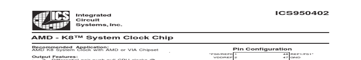
*FS0/REF0 1 VDDREF 2 X1 3 X2 4 GND 5
48 REF1/FS1
* 47 GND 46 VDDREF 45 REF2/FS2
* 44 Reset#
• 4 - Selectable PCICLK/HTTCLK @3.3V
• 1 - 48MHz, @3.3V fixed.
• 1 - 24/48MHz @ 3.3V
• 3 - REF @3.3V, 14.318MHz. Features:
• Programmable output frequency.
*(PCICLK7/HTTCLK0)ModeA 6
*PCICLK8/HTTCLK1/ModeB 7
PCICLK9/HTTCLK2 8 VDDPCI 9 GND 10
PCICLK10/HTTCLK3 11 PCICLK11 12
43 VDDA 42 GND 41 CPUCLK8T0 40 CPUCLK8C0 39 GND 38 VDDCPU 37 CPUCLK8T1
ICS950402
• Programmable output divider ratios.
PCICLK0 13
.

PIN # PIN NAME 1 *FS0/REF0 2 VDDREF 3 X1 4 X2 5 GND 6 *(PCICLK7/HTTCLK0)ModeA 7 *PCICLK8/HTTCLK1/ModeB 8 PCICLK9/HTT.
| No. | Partie # | Fabricant | Description | Fiche Technique |
|---|---|---|---|---|
| 1 | ICS950401 |

Integrated Circuit Systems |
System Clock |

|
| 2 | ICS950401 |

Renesas |
AMD System Clock |
|
| 3 | ICS950403 |
Integrated Circuit Systems |
AMD - K8 System Clock Chip |
|
| 4 | ICS950405 |
Renesas |
System Clock |
|
| 5 | ICS950405 |
Integrated Circuit Systems |
AMD - K8 System Clock Chip |
|
| 6 | ICS950410 |
Integrated Circuit Systems |
AMD - K System Clock Chip |
|
| 7 | ICS950104 |
Integrated Circuit Systems |
Programmable System Clock Chip for PIII Processor |
|
| 8 | ICS950201 |
Renesas |
Programmable Timing Controller |
|
| 9 | ICS950202 |
Integrated Circuit Systems |
Programmable Timing Control Hub |
|
| 10 | ICS950202 |
Renesas |
Programmable Timing Control Hub |
|
| 11 | ICS950208 |
Integrated Circuit Systems |
Programmable Timing Control Hub for P4 |
|
| 12 | ICS950220 |
Renesas |
Programmable Timing Control Hub |
|