
Recherchez avec le numéro de pièce ainsi que le fabricant ou la description
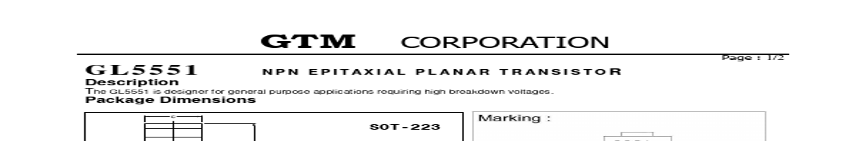
The GL5551 is designer for general purpose applications requiring high breakdown voltages. Package Dimensions Absolute Maximum Ratings at Ta = 25к Parameter Symbol Junction Temperature Tj Storage Temperature Tstg Collector to Base Voltage Collector to Emitter Voltage VCBO VCEO Emitter to Base Voltage VEBO Collector Current IC Total Power Dissip.
=100uA, IE=0 IC=1.0Ma, IB=0 IE=10uA, IC=0 VCB=120V , IE=0 VEB=4V , IC=0 IC=10mA, IB=1.0mA IC=50mA, IB=5mA IC=10mA, IB=1mA IC=50mA, IB=5mA VCE=5V, IC=1mA VCE=5V, IC=10mA VCE=5V, IC=50mA VCE=10V, IC=10mA, f=100MHz VCB=10V, IE=0, f=1MHz Classification Of hFE Rank A Range 80 - 200 N 100 - 250 C 160 - 400 2/2 Characteristics Curve Important Notice: All rights are reserved. Reproduction in whole or in part is prohibited without the prior written approval of GTM. GTM reserves the right to make changes to its products without notice. GTM semiconductor products are not warranted to be suitable .
| No. | Partie # | Fabricant | Description | Fiche Technique |
|---|---|---|---|---|
| 1 | GL5559 |

ETC |
(GL5516 - GL5659D) PHOTO CONDUCTIVE CELL |

|
| 2 | GL55 |

CdS |
Photoresistor |
|
| 3 | GL550 |

Sharp Electrionic Components |
High Speed Infrared Emitting Diode |
|
| 4 | GL551 |
Sharp Electrionic Components |
High Speed Infrared Emitting Diode |
|
| 5 | GL5516 |
ETC |
GL5516 - GL5549 Photoresistor |
|
| 6 | GL5516 |
CdS |
(GL5516 - GL5549) Photoresistor |
|
| 7 | GL5516 |
ETC |
(GL5516 - GL5659D) PHOTO CONDUCTIVE CELL |
|
| 8 | GL5516 |

SENBA |
(GL5516 - GL5549) Photoresistor |
|
| 9 | GL5528 |
ETC |
GL5516 - GL5549 Photoresistor |
|
| 10 | GL5528 |
CdS |
(GL5516 - GL5549) Photoresistor |
|
| 11 | GL5528 |
ETC |
(GL5516 - GL5659D) PHOTO CONDUCTIVE CELL |
|
| 12 | GL5528 |
SENBA |
(GL5516 - GL5549) Photoresistor |
|