
Recherchez avec le numéro de pièce ainsi que le fabricant ou la description
of survivability specs. Semiconductor Components Industries, LLC, 2015 1 February, 2024 − Rev. 8 Publication Order Number: ESD5B5.0ST1/D ESD5B5.0S, SZESD5B5.0S ELECTRICAL CHARACTERISTICS (TA = 25C unless otherwise noted) Symbol Parameter IPP Reverse Peak Pulse Current VC Clamping Voltage @ IPP VRWM Working Peak Reverse Voltage IR Reverse Le.
Low Capacitance 32 pF
Low Clamping Voltage
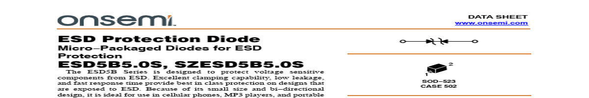
Small Body Outline Dimensions: nom 0.063 x 0.032 (1.6x0.8 mm)
Low Body Height: nom 0.024 (0.6 mm)
Reverse Working (Stand−off) Voltage: 5.0 V
Peak Power up to 50 W @ 8 x 20 ms Pulse
Low Leakage
Response Time is Typically < 1 ns
ESD Rating of Class 3 (> 16 kV) per Human Body Model
IEC61000−4−2 Level 4 ESD Protection
SZ Prefix for Automotive and Other Applications Requiring Unique
Site and Control Change Requirements; AEC−Q101 Qualified and
PPAP Capable
This is a Pb−Free Device
Mechanical Characteristics CASE: Void-free, trans.
| No. | Partie # | Fabricant | Description | Fiche Technique |
|---|---|---|---|---|
| 1 | ESD5B5.0 |

SEMITECH |
Transient Voltage Suppressor |

|
| 2 | ESD5B5.0ST1G |

ON Semiconductor |
Transient Voltage Suppressor Bi-directional Micro-Packaged Diode |
|
| 3 | ESD5B5.0ST1G-N |

BORN |
ESD Protection Diode |
|
| 4 | ESD5B5VL |

WillSEMI |
Small Power TVS |
|
| 5 | ESD5B5WT |

JGD |
Transient Voltage Suppressor |
|
| 6 | ESD5B |
SEMITECH |
Transient Voltage Suppressor |
|
| 7 | ESD5004 |
ON Semiconductor |
ESD Protection Diode |
|
| 8 | ESD5101 |
ON Semiconductor |
ESD Protection Diode |
|
| 9 | ESD5102 |
ON Semiconductor |
ESD Protection Diodes |
|
| 10 | ESD5111 |
ON Semiconductor |
ESD Protection Diode |
|
| 11 | ESD5205 |
ON Semiconductor |
Transient Voltage Suppressors |
|
| 12 | ESD5301N |
WillSEMI |
Small Power TVS |
|