
Recherchez avec le numéro de pièce ainsi que le fabricant ou la description
of survivability specs. Semiconductor Components Industries, LLC, 2017 1 February, 2024 − Rev. 6 Publication Order Number: ESD5371/D ESD5371 ELECTRICAL CHARACTERISTICS (TA = 25C unless otherwise noted) Symbol Parameter IPP Maximum Reverse Peak Pulse Current VC Clamping Voltage @ IPP VRWM Working Peak Reverse Voltage IR Maximum Reverse Leaka.
Low Clamping Voltage
Small Body Outline Dimensions: 0.62 mm x 0.32 mm
Low Body Height: 0.3 mm
Stand−off Voltage: 3.3 V
IEC61000−4−2 Level 4 ESD Protection
These Devices are Pb−Free, Halogen Free/BFR Free and are RoHS
Compliant
Typical Applications
mSD Card Protection
Audio Line
GPIO
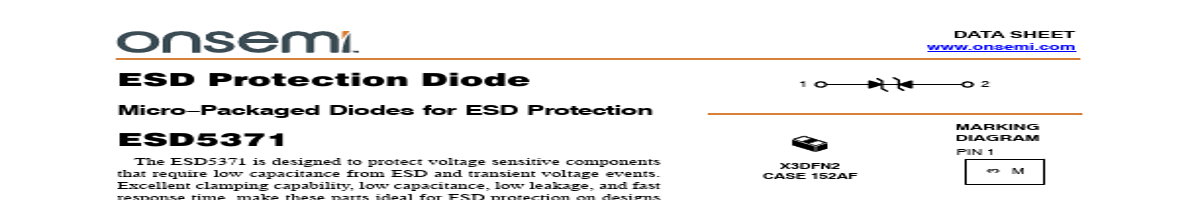
1
2
X3DFN2 CASE 152AF
3
MARKING DIAGRAM PIN 1
M
3 = Specific Device Code M = Date Code
ORDERING INFORMATION
Device
Package Shipping†
ESD5371MXT5G
X3DFN2 10000 / Tape &
(Pb−Free)
Reel
†For information on tape and reel specifications, including part orientation and tape sizes, please r.
| No. | Partie # | Fabricant | Description | Fiche Technique |
|---|---|---|---|---|
| 1 | ESD5374D |

WillSEMI |
Small Power TVS |

|
| 2 | ESD5301N |
WillSEMI |
Small Power TVS |
|
| 3 | ESD5302F |
WillSEMI |
Small Power TVS |
|
| 4 | ESD5302N |
WillSEMI |
Small Power TVS |
|
| 5 | ESD5304D |
WillSEMI |
Small Power TVS |
|
| 6 | ESD5305F |
WillSEMI |
Small Power TVS |
|
| 7 | ESD5305FB |
WillSEMI |
Small Power TVS |
|
| 8 | ESD5306D |
WillSEMI |
Small Power TVS |
|
| 9 | ESD5311N |
WillSEMI |
Small Power TVS |
|
| 10 | ESD5311N-2 |

Leiditech |
TVS Diode |
|
| 11 | ESD5311X |
WillSEMI |
Small Power TVS |
|
| 12 | ESD5311X |
Leiditech |
TVS Diode |
|