
Recherchez avec le numéro de pièce ainsi que le fabricant ou la description
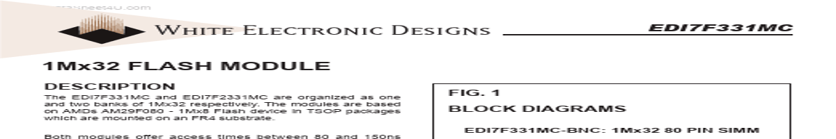
The EDI7F331MC and EDI7F2331MC are organized as one and two banks of 1Mx32 respectively. The modules are based on AMDs AM29F080 - 1Mx8 Flash device in TSOP packages which are mounted on an FR4 substrate. Both modules offer access times between 80 and 150ns allowing for operation of high-speed microprocessors without wait states. EDI7F331MC FIG. 1 BLOCK DIA.
1Mx32 and 2x1Mx32 Densities Based on AMD - AM29F080 Flash Device Fast Read Access Time - 80ns 5V Only Reprogramming Sector Erase Architecture
Uniform sectors of 64 Kbytes each Any combination of sectors can be erased Also supports full chip erase Hardware method that disables any combination of sectors from write or erase operations Automatically preprograms and erases the chip or any combination of sectors Automatically programs and verifies data at specified address
DQ0-DQ7
DQ8-DQ15
DQ16-DQ23
DQ24-DQ31
Sector Protection
Embedded Erase Algorithms
EDI7F2331MC-BNC: .
| No. | Partie # | Fabricant | Description | Fiche Technique |
|---|---|---|---|---|
| 1 | EDI7F331MV |

White Electronic Designs |
1Mx32 FLASH MODULE |

|
| 2 | EDI7F332MC |
White Electronic Designs |
2Mx32 FLASH MODULE |
|
| 3 | EDI7F332MV |
White Electronic Designs |
2Mx32 FLASH MODULE |
|
| 4 | EDI7F33512C |

WEDC |
512Kx32 Flash |
|
| 5 | EDI7F33512V |
White Electronic Designs |
512Kx32 FLASH |
|
| 6 | EDI7F33IMC |

EDI |
1Megx32 Flash Module |
|
| 7 | EDI7F328XDNSN |
White Electronic Designs |
8M x 32 / 2 x 8Mx 32 INTEL J3 BASED |
|
| 8 | EDI7F341MC |
White Electronic Designs |
1Mx32 FLASH MODULE |
|
| 9 | EDI7F341MV |
White Electronic Designs |
1Mx32 FLASH MODULE |
|
| 10 | EDI7F342MC |
White Electronic Designs |
2Mx32 FLASH MODULE |
|
| 11 | EDI7F342MV |
White Electronic Designs |
2Mx32 FLASH MODULE |
|
| 12 | EDI7F34IMC |
EDI |
1Megx32 Flash Module |
|