
Recherchez avec le numéro de pièce ainsi que le fabricant ou la description
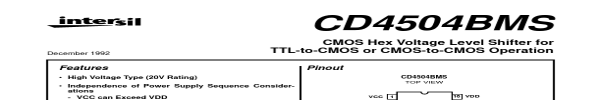
of ‘B’ Series CMOS Devices” VCC 1 16 VDD 15 FOUT 14 FIN 13 SELECT 12 EOUT 11 EIN 10 DOUT 9 DIN AOUT 2 AIN BOUT BIN COUT CIN VSS 3 4 5 6 7 8 Functional Diagram VCC VDD LEVEL SHIFTER OUT (2, 4, 6, 10, 12, 15) Description CD4504BMS hex voltage level shifter consists of six circuits which shift input signals from the VCC logic level to the VDD logic level..
• High Voltage Type (20V Rating)
• Independence of Power Supply Sequence Considerations - VCC can Exceed VDD - Input Signals can Exceed Both VCC and VDD
• Up and Down Level Shifting Capability
• Shiftable Input Threshold for Either CMOS or TTL Compatibility
• 100% Tested for Quiescent Current at 20V
• 5V, 10V and 15V Parametric Ratings
• Standardized Symmetrical Output Characteristics
• Maximum Input Current of 1µA at 18V Over Full Package Temperature Range; 100nA at 18V and +25oC
• Meets All Requirements of JEDEC Tentative Standard No. 13B, “Standard Specifications for Description of ‘B’ Serie.
| No. | Partie # | Fabricant | Description | Fiche Technique |
|---|---|---|---|---|
| 1 | CD4504B |

ETCTI |
CMOS HEX VOLTAGE-LEVEL SHIFTER |

|
| 2 | CD4504B-EP |
ETCTI |
CMOS Hex Voltage-Level Shifter for TTL-to-CMOS or CMOS-to-CMOS Operation |
|
| 3 | CD4504B-MIL |
ETCTI |
CMOS HEX VOLTAGE-LEVEL SHIFTER |
|
| 4 | CD4504BT |

Intersil Corporation |
CMOS Hex Voltage Level Shifter for TTL-to-CMOS or CMOS-to-CMOS Operation |
|
| 5 | CD4502B |
ETCTI |
CMOS Strobed Hex Inverter/Buffer |
|
| 6 | CD4502B |

RCA |
CMOS Strobed Hex Inverter/Buffer |
|
| 7 | CD4502B-MIL |
ETCTI |
CMOS Strobed Hex Inverter/Buffer |
|
| 8 | CD4502BMS |
Intersil Corporation |
CMOS Strobed Hex Inverter/Buffer |
|
| 9 | CD4503B |
ETCTI |
CMOS HEX BUFFER |
|
| 10 | CD4503B |
RCA |
CMOS HEX BUFFER |
|
| 11 | CD4503BC |

National Semiconductor |
Hex Non-Inverting TRI-STATE Buffer |
|
| 12 | CD4503BC |

Fairchild Semiconductor |
Hex Non-Inverting 3-STATE Buffer |
|