
Recherchez avec le numéro de pièce ainsi que le fabricant ou la description
Reset Vref Vref GND GND Pin No. SMP5C2 EMP5 1 Vout Vout 2 VDD SUB 3 GND NC. 4 NC. GND 5 NC. VDD http://www.Datasheet4U.com Absolute Maximum Ratings (Ta=25˚C) Parameter Power supply voltage CMOS output Power dissipation (SMP5C2) ∗1 Power dissipation (EMP5) ∗2 Symbol VDD – GND VOUT Pd Pd Topr Tstg Output voltage Nch open drain output Operating .
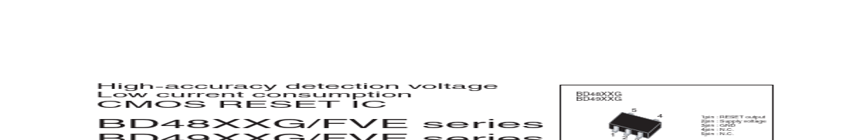
1) Detection voltage: 0.1V step line-up 2.3~6.0V (Typ.) 2) High-accuracy detection voltage:±1.5% Max. 3) Ultra low current consumption: 0.8µA typ. 4) Nch open drain output (BD48XXG/FVE series), CMOS output (BD49XXG/FVE series) 5) Small EMP5, SMP5C2 package Applications Every kind of appliances with microcontroller and logic circuit Application Circuit BD48XXG/FVE VDD VDD VDD VDD BD48XXFVE BD49XXFVE 5 1 2 4 3 1.6±0.05 1.0±0.05 5 4 1pin : RESET output 2pin : SUB Connect to GND 3pin : N.C. 4pin : GND 5pin : Supply voltage 0.2MAX 0.13±0.05 0.08 M 1.6±0.05 1.2±0.05 1 2 3 Lot No. 0.6MAX 0..
| No. | Partie # | Fabricant | Description | Fiche Technique |
|---|---|---|---|---|
| 1 | BD4926 |

Rohm |
CMOS Voltage Detector |

|
| 2 | BD4926FVE |

ETC |
CMOS RESET |
|
| 3 | BD4923 |
Rohm |
CMOS Voltage Detector |
|
| 4 | BD4923FVE |
ETC |
CMOS RESET |
|
| 5 | BD4923FVE |
Rohm |
Voltage Detector |
|
| 6 | BD4923G |
ETC |
CMOS RESET |
|
| 7 | BD4924 |
Rohm |
CMOS Voltage Detector |
|
| 8 | BD4924FVE |
ETC |
CMOS RESET |
|
| 9 | BD4924G |
ETC |
CMOS RESET |
|
| 10 | BD4925 |
Rohm |
CMOS Voltage Detector |
|
| 11 | BD4925FVE |
ETC |
CMOS RESET |
|
| 12 | BD4925G |
ETC |
CMOS RESET |
|