
Recherchez avec le numéro de pièce ainsi que le fabricant ou la description
The ADN4664 is a dual, CMOS, low voltage differential signaling (LVDS) line receiver offering data rates of over 400 Mbps (200 MHz) and ultralow power consumption. It features a flow-through pinout for easy PCB layout and separation of input and output signals. The device accepts low voltage (310 mV typical) differential input signals and converts them to a .
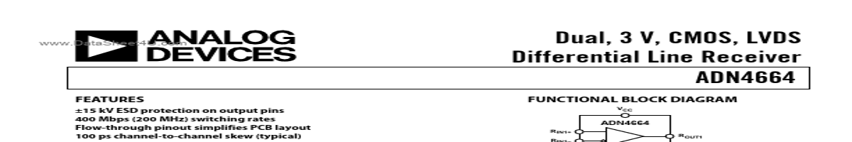
±15 kV ESD protection on output pins 400 Mbps (200 MHz) switching rates Flow-through pinout simplifies PCB layout 100 ps channel-to-channel skew (typical) 2.5 ns maximum propagation delay 3.3 V power supply High impedance outputs on power-down Low power design: typically 3 mW (quiescent) Interoperable with existing 5 V LVDS drivers Accepts small swing (310 mV typical) differential signal levels Supports open, short, and terminated input fail-safe 0 V to −100 mV threshold region Conforms to TIA/EIA-644 LVDS standard Industrial operating temperature range: −40°C to +85°C Available in surface-mou.
| No. | Partie # | Fabricant | Description | Fiche Technique |
|---|---|---|---|---|
| 1 | ADN4661 |

Analog Devices |
High Speed Differential Driver |

|
| 2 | ADN4662 |
Analog Devices |
LVDS Differential Line Receiver |
|
| 3 | ADN4663 |
Analog Devices |
LVDS High Speed Differential Driver |
|
| 4 | ADN4665 |
Analog Devices |
CMOS Differential Line Driver |
|
| 5 | ADN4666 |
Analog Devices |
Quad CMOS Differential Line Receiver |
|
| 6 | ADN4667 |
Analog Devices |
3V LVDS Quad CMOS Differential Line Driver |
|
| 7 | ADN4668 |
Analog Devices |
3V LVDS Quad CMOS Differential Line Receiver |
|
| 8 | ADN4600 |
Analog Devices |
Asynchronous Crosspoint Switch |
|
| 9 | ADN4604 |
Analog Devices |
Digital Crosspoint Switch |
|
| 10 | ADN4605 |
Analog Devices |
4.25 Gbps 40 x 40 Digital Crosspoint Switch |
|
| 11 | ADN4612 |
Analog Devices |
12 x 12 Digital Crosspoint Switch |
|
| 12 | ADN4650 |
Analog Devices |
Dual-Channel LVDS Isolators |
|