
Recherchez avec le numéro de pièce ainsi que le fabricant ou la description
PIN NUMBER 2, 12 3, 11 4, 10 1, 13 5, 9 6, 8 7 14 SYMBOL D0, D1 CP0, CP1 SD0, SD1 RD0, RD1 Q0, Q1 Q0, Q1 GND VCC NAME AND FUNCTION Data inputs Clock inputs (active rising edge) Set inputs (active-Low) Reset inputs (active-Low) Data outputs (active-Low), non-inverting Data outputs (active-Low), inverting Ground (0V) Positive supply voltage DESCRIPTION The 74.
• Metastable immune characteristics
• Pin compatible with 74F74 and 74F5074
• Typical fMAX = 200MHz
• Output skew guaranteed less than 2.0ns
• High source current (IOH = 15mA) ideal for clock driver
applications
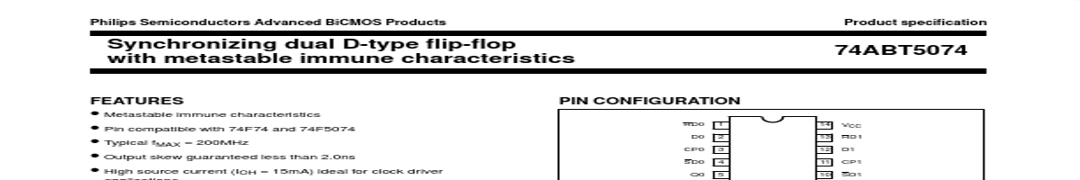
PIN CONFIGURATION
RD0 D0 CP0 SD0 Q0 Q0 GND 1 2 3 4 5 6 7 14 13 12 11 10 9 8 VCC RD1 D1 CP1 SD1 Q1 Q1
• Output capability: +20mA/
–15mA
• Latch-up protection exceeds 500mA per Jedec JC40.2 Std 17
• ESD protection exceeds 2000V per MIL STD 883 Method 3015
and 200V per Machine Model
SA00001
PIN DESCRIPTION
PIN NUMBER 2, 12 3, 11 4, 10 1, 13 5, 9 6, 8 7 14 SYMBOL D0, D1 CP0, CP1 SD0, S.
| No. | Partie # | Fabricant | Description | Fiche Technique |
|---|---|---|---|---|
| 1 | 74ABT534A |

NXP |
Octal D-type flip-flop |

|
| 2 | 74ABT540 |
NXP |
Octal buffer |
|
| 3 | 74ABT541 |
NXP |
Octal buffer/line driver |
|
| 4 | 74ABT541 |

Fairchild Semiconductor |
Octal Buffer/Line Driver |
|
| 5 | 74ABT543 |
Fairchild Semiconductor |
Octal Registered Transceiver |
|
| 6 | 74ABT543A |
NXP |
Octal latched transceiver |
|
| 7 | 74ABT543AD |
NXP |
Octal latched transceiver |
|
| 8 | 74ABT543ADB |
NXP |
Octal latched transceiver |
|
| 9 | 74ABT543APW |
NXP |
Octal latched transceiver |
|
| 10 | 74ABT544 |
NXP |
Octal latched transceiver |
|
| 11 | 74ABT544D |
NXP |
Octal latched transceiver |
|
| 12 | 74ABT544DB |
NXP |
Octal latched transceiver |
|