
Recherchez avec le numéro de pièce ainsi que le fabricant ou la description
PIN NUMBER 1, 2, 4, 5, 9, 10, 12, 13 6, 8 7 14 SYMBOL An, Bn, Cn, Dn Yn GND VCC NAME AND FUNCTION SF00068 Data inputs Data outputs Ground (0V) Positive supply voltage FUNCTION TABLE INPUTS An L X X X Bn X L X X Cn X X L X H Dn X X X L H OUTPUT Yn H H H H L LOGIC SYMBOL 1 2 4 5 9 10 12 13 A0 B0 C0 D0 A1 B1 C1 D1 Y0 Y1 VCC = Pin 14 GND = Pin 7 6 8 .
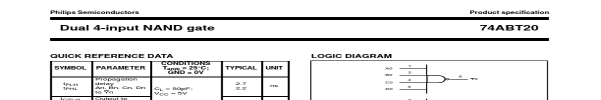
Y1 VCC = Pin 14 GND = Pin 7 6 8
H H NOTES: H = High voltage level L = Low voltage level X = Don’t care
SA00351
ORDERING INFORMATION
PACKAGES 14-Pin Plastic DIP 14-Pin plastic SO 14-Pin Plastic SSOP Type II 14-Pin Plastic TSSOP Type I TEMPERATURE RANGE
–40°C to +85°C
–40°C to +85°C
–40°C to +85°C
–40°C to +85°C OUTSIDE NORTH AMERICA 74ABT20 N 74ABT20 D 74ABT20 DB 74ABT20 PW NORTH AMERICA 74ABT20 N 74ABT20 D 74ABT20 DB 74ABT20PW DH DWG NUMBER SOT27-1 SOT108-1 SOT337-1 SOT402-1
1995 Sep 22
1
853-1811 15793
Philips Semiconductors
Product specification
Dual 4-input NAND gate
74ABT20
ABSO.

The 74ABT20 high-performance BiCMOS device combines low static and dynamic power dissipation with high speed and high o.
| No. | Partie # | Fabricant | Description | Fiche Technique |
|---|---|---|---|---|
| 1 | 74ABT20D |

nexperia |
Dual 4-input NAND gate |

|
| 2 | 74ABT20DB |
nexperia |
Dual 4-input NAND gate |
|
| 3 | 74ABT20PW |
nexperia |
Dual 4-input NAND gate |
|
| 4 | 74ABT2240 |

NXP |
Octal inverting buffer |
|
| 5 | 74ABT2240 |

Fairchild Semiconductor |
Octal Buffer/Line Driver |
|
| 6 | 74ABT2241 |
NXP |
Octal buffers |
|
| 7 | 74ABT2244 |
NXP |
Octal buffer/line driver |
|
| 8 | 74ABT2244 |
Fairchild Semiconductor |
Octal Buffer/Line Driver |
|
| 9 | 74ABT2245 |
NXP |
Octal transceiver |
|
| 10 | 74ABT240 |
NXP |
Octal inverting buffer |
|
| 11 | 74ABT240 |
Fairchild Semiconductor |
Octal Buffer/Line Driver |
|
| 12 | 74ABT241 |
NXP |
Octal buffer/line driver |
|